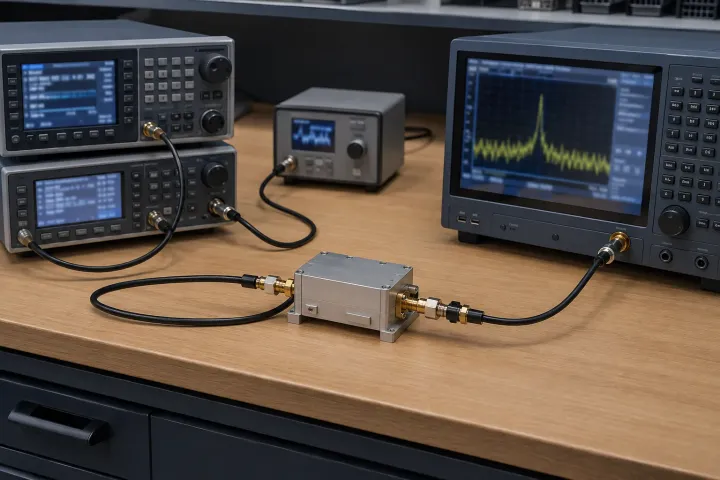
Direct answer
HMC832 lock detect does not prove a stated RF frequency tolerance. The Rev. A data sheet says the function verifies the desired frequency by counting divided-reference and divided-VCO edge pairs that arrive inside a timing window, for the count set in Register 0x07[2:0] (2048 by default). Analog Devices' 2021 forum reply calls the frequency highly accurate at that point, notes that output phase may still be settling, and gives no Hz or ppm figure. If your system needs the output within a set offset after a hop, write that tolerance into the test plan and measure the RF output against it.
Key takeaways
- HMC832 lock detect counts consecutive edge pairs inside a timing window at the phase detector; it does not measure RF frequency error.
- Neither the Rev. A data sheet nor ADI's forum reply gives a Hz or ppm tolerance at the moment LD asserts.
- Register 0x07 sets the count and the window; size the window for the actual PD frequency, charge-pump settings and mode.
- Trigger the RF capture from the hop command and keep the LD result and the RF result in separate fields.
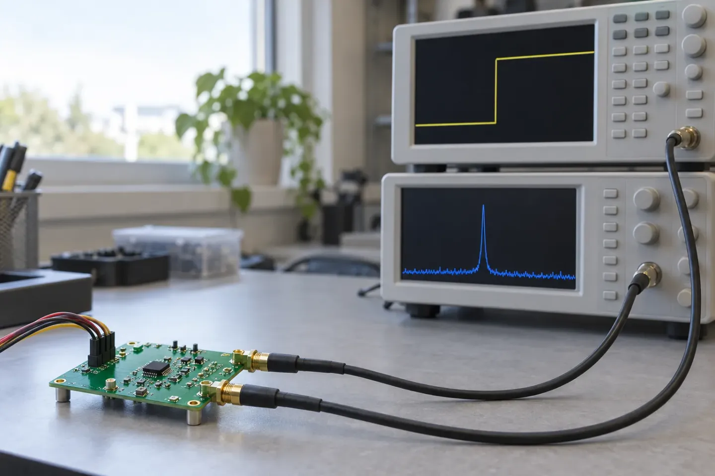
When an HMC832 asserts lock detect (LD) after a frequency change, the Rev. A data sheet says that function verifies the part is generating the desired frequency. The circuit does this by counting divided-reference and divided-VCO edge pairs that arrive inside a timing window. The data sheet attaches no frequency tolerance, in hertz or ppm, to that event. If your system needs the RF output within a stated offset after a hop, put that tolerance in the test plan and measure the output against it.
This guide is for engineers validating HMC832 hops. It reads the Rev. A data sheet’s lock-detect section, ADI’s 2021 answer to this exact question and two measurement references, then gives a record you can copy into a test plan. It belongs to the site’s RF engineering guides. For the loop behaviour that leads up to lock, see the lock transient in our PLL synthesizer guide.
What the HMC832 lock detector checks
The HMC832 data sheet, Rev. A, page 23 describes the circuit. The divided VCO edge and the divided reference edge must arrive at the phase detector within a user-set window, repeatedly; either edge may arrive first, and only the difference in arrival time matters. Each in-window pair increments an internal counter. When the count reaches and exceeds the value set in Register 0x07[2:0], the part declares lock. One pair outside the window resets the counter and declares unlock immediately. Writing Register 0x07[3] = 1 enables the function.
![Flow diagram: with 0x07[3] set, divided reference and divided VCO edges are compared at the phase detector; in-window pairs increment a counter, a miss resets it and declares unlock, reaching the 0x07[2:0] count declares lock, checking continues after lock, and the result appears in register 0x12[1] and, when routed by 0x0F, on the LD_SDO pin](/images/editorial/hmc832-lock-detect-frequency-tolerance/lock-detect-logic.svg)
The result is available in two places. Register 0x12[1] reads 1 when locked and 0 when unlocked. The LD_SDO pin can carry the flag once Register 0x0F[7] = 1 and Register 0x0F[4:0] = 1, but that pin is shared with serial data out: during an SPI read it switches to SDO and returns to LD when the read completes. Setting Register 0x0F[6] = 1 keeps LD on the pin and gives up readback (data sheet page 24).
Common mistake: Logging a drop on the LD_SDO pin as loss of lock when it coincides with an SPI register read. During the read the pin carries SDO; check the read timing, or read Register 0x12[1], before recording an unlock.
The detector’s inputs are the divided signals at the phase detector frequency. The data sheet’s check is that edge timing, not a comparison of the RF output against a frequency standard, so the RF frequency error is a separate measurement.
Takeaway: Treat LD as a phase-detector timing flag and plan a separate RF frequency measurement.
Which register fields change the indication
Register 0x07 holds the lock-detect settings. The defaults below come from Table 21 (data sheet page 38, default word 0x00014D); the window values come from Table 9, which the data sheet labels typical and lists as nominal.
| Field | What it sets | Rev. A default | What a change alters | What it does not tell you |
|---|---|---|---|---|
| 0x07[3] | Internal lock detect enable | 1 (enabled) | Whether LD runs at all | Anything about the RF output |
| 0x07[2:0] | Consecutive in-window count before lock: codes 0 to 7 give 5, 32, 96, 256, 512, 2048, 8192 and 65,535 | Code 5, 2048 counts | How long a clean run must last before LD asserts | A settling time or a frequency error |
| 0x07[6] | Window type: 0 is an analog one-shot with a nominal 10 ns window; 1 is a digital programmable window | 1 (digital) | Fixed or programmable window | Whether that window suits your operating point |
| 0x07[11:10] and 0x07[9:7] | Digital window timer speed and duration setting; Table 9 spans 6.5 to 338 ns nominal | 00 and 010, which Table 9 lists as 11 ns nominal | How far apart the two edges may arrive and still count | A guaranteed window width |
| 0x07[13] | Automatic relock: reruns VCO calibration and tries to relock once if LD reports unlock | 0 (off) | What the part does after an LD failure | Whether the relocked output met your tolerance |
| 0x0F[7], 0x0F[4:0], 0x0F[6] | Routing of the LD flag to the LD_SDO pin | See page 24 | Whether the pin shows LD, and whether readback survives | Lock state during an SPI read |
The window has to suit the operating point. In fractional mode, the data sheet’s Equation 10 calculates the required window from the phase detector frequency, the charge-pump current and the charge-pump offset current. In integer mode, Equation 11 is:
LD window (s) = 1 / (2 × f_PD)If Equation 10 gives 10 ns, the analog detector can be used; otherwise the data sheet calls for the digital window, set to the nearest Table 9 entry. Its own example assumes fractional mode, a 50 MHz phase detector, 2 mA charge-pump gain and a +400 µA offset, and arrives at 13.33 ns, which maps to the 13.3 ns entry. That is a worked example, not a recommended setting. The data sheet adds that one solution does not fit every operating point: a significant change in phase detector frequency or charge-pump offset may need a different window. Integer mode runs with the charge-pump offset disabled (page 22), so record the mode alongside the register values.
Takeaway: Record the 0x07 readback with the phase detector frequency, charge-pump settings and mode, because the window only means something at that operating point.
Does LD high give a frequency tolerance?
The data sheet and ADI’s forum reply do not give one. In December 2021 an engineer asked on ADI’s EngineerZone forum what frequency offset remains at the instant LD goes high, and whether the LD registers change it. ADI’s reply says the frequency “should be highly accurate” once the divided edges stay in the same window for the configured count, 2048 by default, while the output phase “may drift back and forth or drift in one direction a little” as it settles. Raising the count makes LD take longer, and the reply expects frequency and phase accuracy to improve with it. Shrinking the digital window makes LD harder to indicate and, the reply warns, can make it fail at temperature extremes. The reply gives no Hz or ppm value, and the data sheet adds none.
ADI’s AN-873 shows the same separation on a different family. It covers the ADF4xxx integer-N synthesizers and the ADF4360-x parts, and states that their digital lock detect declares lock before the PLL has settled to final frequency and phase. Its simulated 35 MHz jump shows the digital indicator going high about 150 µs before lock. Those numbers belong to that family and that simulation, not to the HMC832. What carries over is narrower: a digital lock indication and final frequency settling are separate events, and a test plan should not assume they coincide.
Write the RF requirement as its own line: target frequency, allowed error in Hz or ppm, when after the hop command it applies, and how long the output must stay inside it. The synthesizer specification table keeps settling tolerance as its own entry. If phase, spurs or noise also matter at that moment, give each its own criterion; the phase noise guide covers how offset and carrier conditions change that number. When the HMC832 drives a mixer as the local oscillator, its frequency error moves the IF by the same amount in a single-conversion plan (RF, IF and LO explained), so derive the tolerance from what the downstream channel can absorb.
Takeaway: Write the RF tolerance, its start time after the command and its hold time into the test plan; do not infer them from LD.
How to capture LD and RF frequency for one hop
The steps below combine the HMC832 data sheet with Tektronix’s PLL characterization note. That note describes characterizing an integrated PLL from the signals you can reach (output, reference and control inputs), triggering a real-time spectrum analyzer either from a control signal or with a frequency mask trigger, and keeping pre-trigger and post-trigger data so the whole frequency trajectory is visible.
- Read back Registers 0x07, 0x09 and 0x0A and record them with the phase detector frequency, the mode and the part marking.
- Note whether VCO autocalibration runs on the frequency write. With Register 0x0A[11] = 0 it starts automatically on every frequency change (data sheet page 18). Note whether automatic relock, 0x07[13], is on. Both fall inside the interval you are timing.
- Trigger the capture from the controller’s frequency write, not from LD, and keep enough pre-trigger data to see the starting frequency.
- Capture LD on an input that shares the RF capture’s time base, such as a spare channel or trigger input on the same instrument. If LD goes to a separate logic analyzer or oscilloscope, send the same hop-command marker to both instruments and measure and correct the offset between their trigger points, including cable and processing delays. Avoid SPI reads during the capture window, or set 0x0F[6] for the test and record that you did.
- On that aligned time base, record when LD asserts and when the RF output enters your tolerance and stays there. Tektronix states its own example result as settling “to within 100 kHz of the final frequency”; that figure belongs to the PLL in their note, but the form is the one to copy, since a settling time without a tolerance is incomplete.
- Repeat at the hop endpoints, supply and temperature corners the system will see. ADI’s caution about window size at temperature extremes is the reason to include the corners.
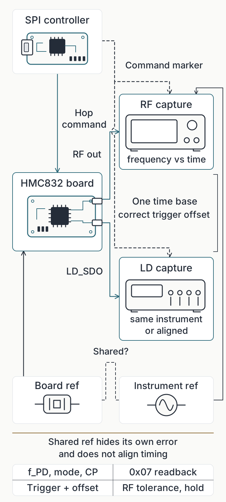
Common mistake: Triggering the RF capture from LD. Time zero is then the event under test: settling is no longer timed from the hop command, and a hop in which LD never asserts produces no capture.
Decide what the frequency measurement is referenced to. If the analyzer and the HMC832 board share one reference, the capture shows the loop tracking that reference but cannot show the reference’s own error. Where absolute frequency matters, reference the instrument independently or carry the shared reference’s accuracy into the result, and write down the measurement uncertainty. This is general measurement practice, not a reported HMC832 result; this site does not test hardware, as its sources and methodology page states. A shared frequency reference and a shared time base are separate questions: connecting the board and the instrument to one reference does not align the trigger times of two instruments, and aligning the triggers does not fix the frequency error.
Takeaway: Start the capture from the hop command, put LD and RF on one aligned time base, and state what the frequency reading is referenced to.
Hop acceptance record
Use one record per hop and condition. Leave a field blank or mark it unknown rather than filling it from the LD flag. Confirm the part marking against the exact data sheet revision before relying on any bit position; the obsolete RF component sourcing guide covers marking and revision checks.
| Group | Field | Entry |
|---|---|---|
| Identity | Part marking; data sheet and revision used | |
| Operating point | Reference source, frequency and stated accuracy | |
| Operating point | R divider, phase detector frequency, integer or fractional mode | |
| Operating point | Charge-pump current and offset (0x09 readback) | |
| LD configuration | 0x07 readback: count code, window type, timer speed and duration | |
| LD configuration | Window from Equation 10 or 11, and the Table 9 entry chosen | |
| LD configuration | Autocalibration (0x0A[11]) and automatic relock (0x07[13]) state | |
| Hop | Start frequency, target frequency, output divider setting | |
| Hop | Trigger source and pre-trigger length | |
| Measurement | Instrument, its frequency reference, measurement uncertainty | |
| Measurement | LD capture input and how it is time-aligned to the RF capture | |
| RF criterion | Allowed error (Hz or ppm), window after the command, hold time | |
| RF criterion | Phase, spur or noise criteria, if any | |
| Conditions | Temperature, supply, any SPI reads during capture | |
| Result | LD asserted? Time from command | |
| Result | RF entered and held tolerance? Time from command | |
| Verdict | RF acceptance: pass, fail or indeterminate |
Keep the two results apart. Judge RF acceptance at the point the plan defines: the hop passes if the RF output is inside tolerance by the stated time after the command and stays inside for the hold time, and fails if it is not. An excursion before that time is recorded but is not a fail on its own, and the LD state does not change the RF verdict in either direction. Log when LD asserted as a separate event. RF inside tolerance without a stable LD flag means the LD window or count needs checking against Equation 10 or 11 for that operating point before you rely on the flag in production. A capture that lacks the trigger, the time alignment, the reference or the stated tolerance, or whose measurement uncertainty is too large to decide against that tolerance, is indeterminate, whatever the trace looks like.
Takeaway: Give the RF verdict from the tolerance, time window and hold time alone, and report the LD event beside it.
When this does not apply
Every register position here comes from the HMC832 Rev. A data sheet. The HMC832A and the HMC830 are separate parts with their own documents; check the data sheet for the part on your board rather than carrying these bit positions across. The forum reply and the data sheet are both qualitative about frequency accuracy at LD, so this page gives no tolerance number, and none of its tables are measurements.
Takeaway: Check the data sheet for the part and revision on your board before reusing any bit position from this page.
For the loop behaviour behind the indication, go back to how frequency synthesizers work. For the full list of synthesizer specifications, see the microwave synthesizer guide, and for matching test conditions across datasheets, the engineering comparison checklist. The wider set of RF component guides covers the surrounding hardware. Corrections follow our editorial policy.
Frequently asked questions
What is the frequency tolerance when HMC832 lock detect goes high after tuning to a new frequency?
Neither the HMC832 Rev. A data sheet nor ADI's December 2021 forum reply gives one. LD asserts after the divided reference and divided VCO edges land inside the lock-detect window for the count in Register 0x07[2:0], 2048 by default. ADI describes the frequency as highly accurate at that point while output phase may still be settling. Specify your own RF tolerance and measure the output against it.
Does the HMC832 lock-detect register configuration change the frequency tolerance?
It changes when LD asserts; neither the data sheet nor ADI's reply gives a tolerance for it to change. A higher 0x07[2:0] count needs a longer clean run, and ADI's reply expects frequency and phase accuracy to improve with it, without a number. A smaller digital window makes LD harder to indicate and can make it fail at temperature extremes. The window must also suit PD frequency, charge-pump settings and mode.
Sources
- HMC832 data sheet, Rev. A: pp. 18, 22-24 and 38 (Lock Detect, Table 9, Table 21) — Analog Devices Accessed October 11, 2026.
- HMC832: Frequency tolerance corresponding to lock detect signal (EngineerZone, Dec. 21, 2021) — Analog Devices EngineerZone Accessed October 11, 2026.
- AN-873: Lock Detect on the ADF4xxx Family of PLL Synthesizers, General Performance — Analog Devices Accessed October 11, 2026.
- Characterizing Phase Locked Loops Using Tektronix Real-Time Spectrum Analyzers, Figures 16-18 — Tektronix Accessed October 8, 2026.