Direct answer
At series resonant frequency, an RF or microwave chip capacitor has zero net reactance and its impedance equals a small effective series resistance, generally on the order of 100 milliohms at 1 GHz for high-Q ceramic chips. Exceeding series resonance makes net impedance inductive, which broadband DC blocking and coupling stages usually tolerate while bypass and matching networks require checking parasitic inductance. Edge mounting with electrodes normal to the ground plane suppresses odd-order parallel resonances, whereas flat mounting with electrodes parallel to the ground plane lowers net inductance for bypassing on boards of 25 mils or less. Under EEE-INST-002, ceramic styles CCR, CKS, CKR, and CDR apply a 0.60 voltage derating factor on peak AC ripple plus DC polarizing voltage up to 110 °C, and below 10 Vdc styles CCR, CKR, and CDR carry a 100 Vdc minimum rating.
Key takeaways
- At series resonance, inductive and capacitive reactance magnitudes match and impedance drops to milliohm-level ESR, whereas parallel resonance raises impedance sharply.
- At frequencies well below resonance, quality factor Q equals component reactance at that frequency divided by effective series resistance, making Q frequency-dependent.
- In multi-octave DC blocks, X7R chips pack higher capacitance per unit volume than NPO parts, while keeping parallel-resonance notches under 0.1 dB prevents visible S21 dips.
- Under MIL-PRF-55681F paragraph 3.8, maximum dissipation factor is 0.05 percent for BG, 0.15 percent for BP, and 2.5 percent across BR, BX, and BZ.
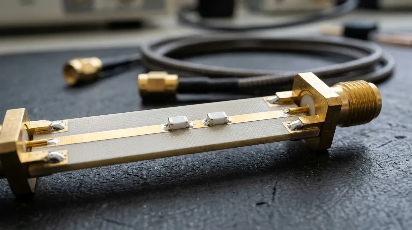
RF microwave capacitors behave as capacitors only below series self-resonance, because alternating current through the part generates series inductance Ls in the structure and leads, effective series resistance ESR in the plates and leads, and solder-pad shunt capacitance Cp from the mounting pads to the ground plane. At series resonant frequency FSR, net reactance vanishes and terminal impedance reaches its minimum ESR floor, generally on the order of 100 milliohms at 1 GHz for high-Q ceramic chip capacitors, whereas higher-frequency parallel resonances at FPR drive impedance sharply upward and carve attenuation notches into passband transmission.
Browse the RF and microwave components hub for selection guides organized by signal-chain function and specification method. In heterodyne hardware where RF sits at the antenna, IF is processed by the rest of the radio, and the LO tone translates between them as detailed in RF, IF, and LO frequency planning, chip capacitors handle interstage DC blocking, bias decoupling, and resonator matching across the low-noise receive downconversion and high-power transmit upconversion chains of an RF module transmitter and receiver.
What Is a Capacitor’s Self-Resonant Frequency (SRF)?
A capacitor’s self-resonant frequency is the natural frequency above which the component starts behaving like an inductor rather than a capacitor. Larger nominal capacitance values cross into self-resonance at much lower frequencies; in Stanford’s passive-component comparison, a 1 µF capacitor reaches self-resonance far below a 5 pF capacitor.
Self-resonance is unavoidable in any physical package. As UC Berkeley’s high-frequency passive-component laboratory note explains, alternating current flowing through a capacitor generates a magnetic field in the internal structure and leads, which is lumped as a single series inductor Ls in series with the nominal capacitance. Finite electrical conductivity in the metallic plates and leads introduces series loss Rs, also called effective series resistance (ESR), while loss in the dielectric between the plates is represented by a large shunt resistance Rdi. Once the chip is soldered onto a printed circuit board, electric fields between the mounting pads and the underlying ground plane add shunt parasitic capacitors Cp at the terminals.
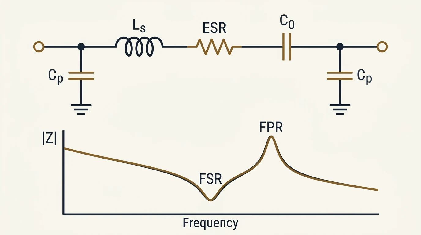
UC Santa Barbara’s broadband-capacitor course note distinguishes two resonant points across frequency:
- Series resonant frequency (FSR), referred to simply as self-resonance, occurs where net reactance drops to zero and the trace crosses the real axis on an S11 Smith chart. For high-Q ceramic chip capacitors, that series-resonant impedance equals a small ESR generally on the order of 100 milliohms at 1 GHz, forming the lowest-impedance path available for coupling or bypassing. At FSR, the magnitudes of inductive reactance XL and capacitive reactance XC are equal, so the impedance magnitude expression √((ESR)² + (XL − XC)²) simplifies directly to that milliohm-scale ESR because the reactance difference XL − XC is zero.
- Parallel resonant frequency (FPR) occurs higher in frequency, where device impedance can become precipitously high, particularly in high-Q parts. For edge-mounted multilayer ceramic capacitors, FPR usually falls at more than twice FSR, and terminal impedance at that point is typically high and inductive.
How Do Q Factor and ESR Behave Below and At Resonance?
At frequencies well below self-resonance, UC Berkeley’s passive-component laboratory note defines quality factor Q as the reactance of the capacitor at the operating frequency divided by Rx, where Rx is the component’s effective series resistance (ESR), making Q an explicit function of frequency. NIST Technical Note 2255 (July 2023) defines radial frequency by ω = 2πf with frequency f in Hz.
UC Santa Barbara’s resonator course note defines capacitor unloaded quality factor QU from its isolated series equivalent network of capacitive reactance X and series resistance R, independent of external circuit loading. Higher unloaded Q indicates lower internal power dissipation, and capacitor unloaded Q decreases as frequency increases.
Component datasheets and procurement standards treat ESR differently depending on dielectric technology and frequency band:
- High-Q microwave ceramic chips reach milliohm-scale series resistance near self-resonance, described in the UC Santa Barbara broadband-capacitor note as generally on the order of 100 milliohms at 1 GHz.
- Under military specification MIL-PRF-55681F (paragraphs 3.10 and 3.11), ceramic multilayer chip capacitors undergo UHF ESR testing (per 4.8.7) and RF ESR testing (per 4.8.8) when specified by the detail specification, with maximum allowable ESR bounded by the curves in Appendix A of that document.
- EEE-INST-002 Table 4 Note 4 sets the ESR floor on solid-tantalum styles CSR, CSS, and CWR. Grade 2 requires ESR of at least 0.1 ohms per volt or 1 ohm, whichever is greater, and Grade 1 requires at least 0.3 ohms per volt or 1 ohm, whichever is greater.
DC Block vs. RF Bypass: Why Do Notches Appear on S21?
Exceeding series resonant frequency FSR makes a capacitor’s net impedance inductive, which the UC Santa Barbara broadband-capacitor note observes is usually acceptable for broadband DC blocking and AC coupling, whereas RF bypass and impedance-matching circuits must evaluate net impedance and parasitic inductance carefully. For narrowband RF bypassing on bias lines, select a chip whose series resonant frequency FSR sits at or close to the desired bypass frequency so the (XL − XC) term vanishes and shunt impedance equals ESR.
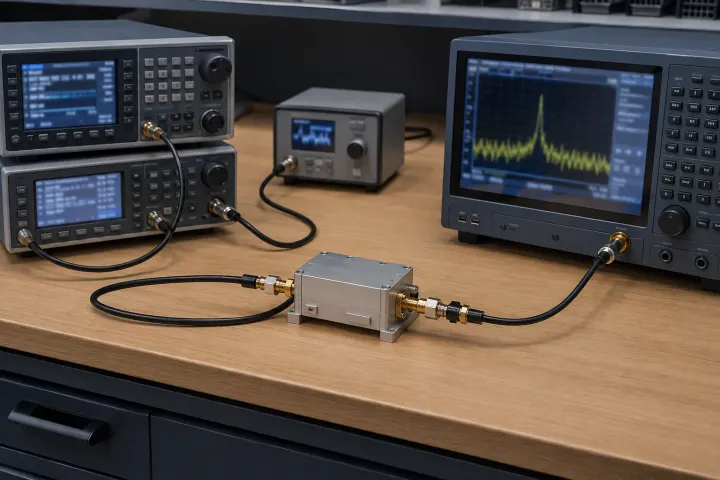
In broadband series coupling and DC-block stages, insertion loss across the passband is verified through two-port scattering parameters (S-parameters), which NIST’s calibrated scattering-parameter technical note defines as unitless ratios of wave parameters measured on one-port and two-port coaxial or waveguide artifacts using a vector network analyzer (VNA) with traceable calibration artifacts. When preparing coaxial test fixtures and documenting bench setups, pair VNA calibration checks with the SMA connector torque and pin-depth guide, RF-to-IF isolation measurement conditions, and the broader RF engineering measurement guides.
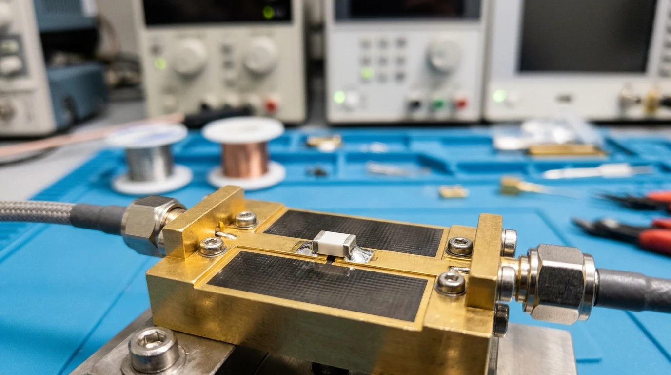
Examining the magnitude of S21 across frequency exposes any parallel resonances falling inside the operating band as distinct attenuation notches, while overall insertion loss of several tenths of a dB is generally acceptable across typical passbands. Counterintuitively, very low ESR worsens passband notches when a broadband DC block operates far above FSR and near FPR:
- Low series resistance RS in the parasitic branch produces high terminal impedance at FPR, carving a deep attenuation notch into S21.
- Higher series resistance RS lowers the parallel-resonant impedance at FPR and yields a much shallower attenuation dip. When high loss at FPR holds notch depth below 0.1 dB, the dip becomes indiscernible on the magnitude of S21, satisfying the broadband single-capacitor DC-block criterion.
- In a flat-mount series-through measurement with internal electrodes parallel to the substrate, the UC Santa Barbara broadband-capacitor note documents a 10 nF capacitor maintaining less than 0.5 dB insertion loss across the entire plotted span from 50 MHz to 4 GHz.
| Circuit Application | Operating Frequency vs. FSR | ESR & Parallel Resonance (FPR) Goal | Preferred Mounting Orientation | Typical Ceramic Dielectric Choice |
|---|---|---|---|---|
| Broadband DC block and series AC coupling | Operating above FSR (inductive net impedance) is usually acceptable across multi-octave bands | Keep passband S21 loss within a few tenths of a dB; higher loss at FPR can flatten parallel-resonance notches under 0.1 dB | Edge mounting (electrodes normal to ground plane) to suppress odd-order parallel resonances | X7R for higher capacitance per unit volume than NPO across multi-octave low-frequency edges |
| Narrowband RF supply bypass | Place FSR at or close to the target bypass frequency where net reactance is zero | Low milliohm ESR at FSR (on the order of 100 milliohms at 1 GHz for high-Q ceramic chips) sets minimum shunt impedance | Flat mounting (electrodes parallel to ground plane) on boards of 25 mils or less to lower net inductance | High-Q ceramic chip sized so FSR aligns with the target RF tone |
| Impedance matching, filters, and resonators | Operate well below FSR where behavior remains predictably capacitive and parasitic inductance is accounted for | Maximize unloaded Q (reactance divided by ESR) to minimize insertion loss in filters and amplifiers | Consistent pad geometry keeping shunt pad capacitance Cp and lead inductance Ls repeatable | Class I COG (BP) temperature-stable ceramic over Class II X7R (BX) |
Does Flat vs. Edge Mounting Shift SRF and Parallel Resonance?
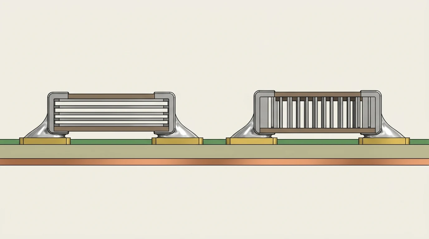
Mounting orientation and substrate thickness alter both the net parasitic inductance and the harmonic modal behavior of multilayer ceramic chip capacitors on microstrip lines. The UC Santa Barbara broadband-capacitor note compares the two standard solder orientations relative to the PCB ground plane:
- Edge mounting (vertical orientation) places the internal metallic electrodes normal to the ground plane. Rotating the electrode stack perpendicular to the board greatly suppresses odd-order parallel resonances in wideband series transmission paths. For edge-mounted multilayer ceramic capacitors, parallel resonance FPR usually lies above twice FSR.
- Flat mounting (horizontal orientation) places the internal electrodes parallel to the ground plane. Keeping the bottom plates close and parallel to the return plane yields lower net parasitic inductance and a somewhat higher series resonant frequency FSR, making flat mounting advantageous in RF bypass circuits.
- Substrate thickness directly governs return-path loop area; boards on the order of 25 mils or less are preferred to keep the mounted chip close to the ground plane when minimizing net inductance.
Layout and Selection Rules of Thumb
- When decoupling a narrowband RF rail or local-oscillator feed, choose a capacitor value and package whose series resonant frequency FSR sits at or near the target bypass frequency and mount it flat on a substrate of 25 mils or less to minimize loop inductance.
- When coupling a multi-octave microwave signal path above FSR where odd-order parallel resonances threaten S21 flatness, specify edge mounting with internal electrodes normal to the ground plane, or verify on a VNA that higher loss near FPR damps any in-band notch below 0.1 dB.
- When the operating bias is under 10 Vdc, specify ceramic styles CCR, CKR, or CDR with a rating of at least 100 Vdc.
Class I COG (BP) vs. Class II X7R (BX) and Voltage Derating
Dielectric class groups these ceramic chip capacitors before the temperature and voltage limits in the tables below. NASA’s mechanical study of multilayer ceramic capacitors pairs commercial Class I COG (BP) dielectrics against Class II X7R (BX) dielectrics.
Under MIL-PRF-55681F (September 3, 2004), general requirements cover both established-reliability and non-established-reliability ceramic dielectric multiple-layer chip capacitors. In its rating code, first letter B specifies an operating temperature range of -55 °C to +125 °C:
- In MIL-PRF-55681F Table I, voltage-temperature symbol P holds capacitance drift within 0 ± 30 ppm/°C across temperature both at zero bias and at 100 percent of rated voltage, while symbol G specifies 90 ± 20 ppm/°C. NASA NEPP’s MIL-PRF-55681 part-number guide similarly summarizes BP as 0 +/- 30 ppm/°C and BX as +/- 15%.
- In MIL-PRF-55681F Table I, voltage-temperature symbol X permits ± 15 percent capacitance change on zero-voltage temperature steps and shifts to +15, -25 percent at 100 percent of rated voltage. Under MIL-PRF-55681F paragraph 3.8, dissipation factor is capped at 0.05 percent for BG, 0.15 percent for BP, and 2.5 percent across characteristics BR, BX, and BZ.
- An X7R chip may outperform an NPO chip in multi-octave DC-block applications because X7R delivers more capacitance per unit volume to satisfy the low-frequency reactance demand of a wide band.
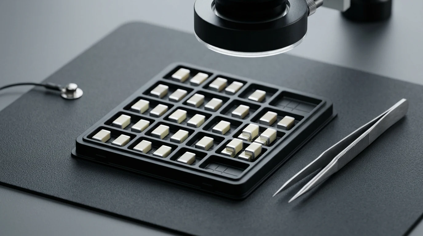
High-reliability RF hardware pairs dielectric selection with electrical and thermal stress derating. NASA GSFC’s EEE-INST-002 (issued May 2003, with Addendum 1 incorporated April 2008) governs EEE parts selection, screening, qualification, and derating. That instruction defines derating as reducing electrical and thermal stresses during normal operation to slow degradation and extend expected life. In its capacitor procurement table, established-reliability chip style CDR references MIL-PRF-55681, while space-level encapsulated and chip style CKS references MIL-PRF-123. NASA NEPP’s MIL-PRF-123 style list identifies CKS05 under MIL-PRF-123/1 as a molded radial-lead style spanning 4.7 pF to 4,700 pF at 100 V.
Compare the governing NASA derating rows and dielectric limits before finalizing part numbers:
| Specification or Guideline | Capacitor Style / Dielectric Row | Voltage & Ripple Derating Rule | Maximum Temperature | Key Limit or Scope Note |
|---|---|---|---|---|
| EEE-INST-002 Table 4 | Ceramic styles CCR, CKS, CKR, CDR | 0.60 factor applied to peak AC ripple plus DC polarizing voltage | 110 °C ambient | Under 10 Vdc operating bias, styles CCR, CKR, and CDR must be rated at least 100 Vdc |
| EEE-INST-002 Table 4 | Plastic-film styles CRH, CHS | 0.60 factor applied to peak AC ripple plus DC polarizing voltage | 85 °C ambient | Lower maximum ambient temperature ceiling than ceramic styles |
| EEE-INST-002 Table 4 Note 4 | Solid-tantalum styles CSR, CSS, CWR | 0.50 factor at 70 °C; 0.30 factor at 110 °C | 70 °C / 110 °C ambient | Requires minimum ESR of 0.1 ohms per volt (Grade 2) or 0.3 ohms per volt (Grade 1), or 1 ohm minimum |
| NASA NEPP Low-Voltage MLCC Guideline | Base-metal-electrode (BME) MLCC row | 0.5 voltage factor on peak AC ripple plus DC polarizing voltage; 0.75 (75%) ripple-current factor | 100 °C operating | Contrasts with MIL 0.6 factor at 110 °C; keep power ripple frequency outside electromechanical resonance |
| MIL-PRF-55681F Table I | Voltage-temperature symbols P and G | 0 ± 30 ppm/°C (symbol P) and 90 ± 20 ppm/°C (symbol G) at 100 percent rated voltage | -55 °C to +125 °C (letter B) | Symbol X allows ± 15 percent at zero bias and +15, -25 percent at 100 percent rated voltage |
| MIL-PRF-55681F Paragraph 3.8 | Characteristics BG, BP, BR, BX, BZ | Measured per 4.8.5 dissipation-factor verification | Specified test temperature | Maximum dissipation factor 0.05 percent (BG), 0.15 percent (BP), and 2.5 percent (BR, BX, BZ) |
In NASA NEPP’s presentation on low-voltage multilayer ceramic capacitors, rated voltage VR is controlled by polarization processes inside the dielectric so that voltage-dependent capacitance and reliability stay within specification limits. When qualifying frequency-translation hardware alongside passive bias and coupling networks, coordinate capacitor derating and S-parameter checks with RF and microwave frequency converters.
Sources
- NASA GSFC EEE-INST-002: Instructions for EEE Parts Selection, Screening, Qualification, and Derating, Incorporating Addendum 1 (May 2003 / April 2008), National Aeronautics and Space Administration, Goddard Space Flight Center.
- Rating and Derating for Low-Voltage MLCCs (2013 NEPP Presentation), NASA Electronic Parts and Packaging (NEPP) Program, Alexander Teverovsky.
- NASA NEPP MIL-PRF-55681 Part-Number Explanation, NASA Parts Selection List (NPSL).
- NASA NEPP MIL-PRF-123 Capacitor Style List, NASA Parts Selection List (NPSL).
- Mechanical Testing of MLCCs, NASA Technical Reports Server.
- High Frequency Passive Components, University of California, Berkeley, Department of Electrical Engineering and Computer Sciences.
- ECE 145A Course Note: Capacitors in Broadband Applications, University of California, Santa Barbara, Department of Electrical and Computer Engineering.
- Resonators and Quality Factor Q, University of California, Santa Barbara, Department of Electrical and Computer Engineering.
- EE133 Handout: Capacitors Demystified, Stanford University, Electrical Engineering.
- NIST Technical Note 2255: Calibrated Scattering-Parameter Measurements (July 2023), National Institute of Standards and Technology.
- U.S. Department of Defense Performance Specification MIL-PRF-55681F, Capacitor, Chip, Multiple Layer, Fixed, Ceramic Dielectric, Established Reliability and Non-Established Reliability, General Specification for, September 3, 2004.
- U.S. Department of Defense Performance Specification MIL-PRF-123, Capacitors, Fixed, Ceramic Dielectric (Temperature Stable and General Purpose), High Reliability, General Specification for.
Frequently asked questions
What is a capacitor's self-resonant frequency?
Self-resonant frequency is the natural crossover frequency above which a real capacitor starts behaving like an inductor, with a 1 µF part crossing over much lower in frequency than a 5 pF chip. At series resonance, net reactance reaches zero and the trace crosses the real axis on an S11 Smith chart, while terminal impedance equals a small ESR generally on the order of 100 milliohms at 1 GHz for high-Q ceramic chips.
Why does a broadband DC-block capacitor create an attenuation notch on S21?
When one or more parallel resonances fall inside the desired passband, they appear on the magnitude of S21 as distinct attenuation notches. At parallel resonant frequency, low series resistance yields high impedance and a deep notch, whereas higher loss at that resonance flattens the notch below 0.1 dB where it becomes indiscernible on S21.
Should you mount an RF multilayer ceramic chip capacitor flat or on edge?
Mount the chip on edge, with internal electrodes normal to the ground plane, when suppressing odd-order parallel resonances across a broadband signal path. Mount the chip flat, with internal electrodes parallel to the ground plane on a board of 25 mils or less, when minimizing net inductance and raising series resonant frequency for RF bypassing.
When does an X7R capacitor outperform a Class I COG or NPO chip at RF?
Across multi-octave DC-blocking spans, an X7R chip provides higher capacitance per unit volume than an NPO chip, meeting low-frequency reactance needs in a compact footprint. Where tight thermal drift governs tuned circuits across -55 °C to +125 °C, MIL-PRF-55681F Table I holds symbol P to 0 ± 30 ppm/°C at 100 percent rated voltage while symbol X shifts to +15, -25 percent. Paragraph 3.8 separately caps dissipation factor at 0.15 percent for BP versus 2.5 percent for BX.