Direct answer
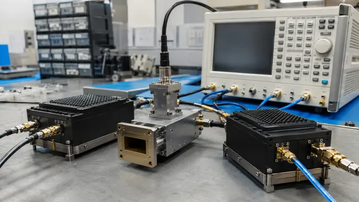
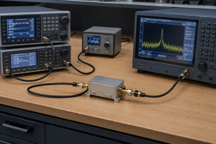
An RF module transmitter and receiver (T/R module) integrates a low-noise receive downconversion chain (preselector, LNA, digital step attenuator, mixer, local oscillator, IF filter, and ADC) with a high-power transmit upconversion chain (DAC, upconverter mixer, spur bandpass filter, driver, and GaN or GaAs power amplifier). Receiver sensitivity and linearity are governed by two competing cascade equations: the Friis noise factor equation F_total = F_1 + (F_2 - 1)/G_1 + (F_3 - 1)/(G_1·G_2) + ..., which favors high pre-mixer LNA gain, and the cascaded third-order intercept equation 1/IIP3_total = 1/IIP3_1 + G_1/IIP3_2 + (G_1·G_2)/IIP3_3 + ..., where excessive pre-mixer gain overdrives the downconversion mixer and collapses two-tone Spurious-Free Dynamic Range (SFDR = (2/3)·(IIP3_total - Noise_Floor)).
Key takeaways
- Pre-LNA passive insertion loss (preselector, T/R switch, limiter) adds dB-for-dB to NF_total, while the first LNA (1.1 dB NF, 19.5 dB gain HMC8410) suppresses the 25–32 dB noise figure of downstream IF and ADC stages.
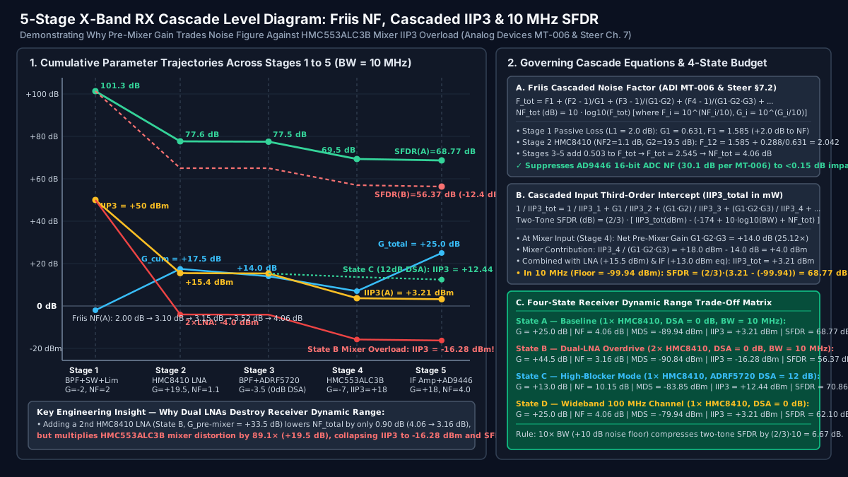
- In our 5-stage X-band receiver, adding a second HMC8410 LNA (+39 dB total LNA gain) lowers NF_total by only 0.90 dB (4.06 to 3.16 dB) while collapsing mixer-limited IIP3_total from +3.21 dBm to -16.28 dBm (-12.40 dB SFDR loss).
- Stepping an interstage ADRF5720 digital step attenuator to 12 dB in high-blocker environments shifts cascaded IIP3_total up to +12.44 dBm and raises 10 MHz SFDR to 70.86 dB at the cost of +6.09 dB higher noise figure.
- Passive double-balanced upconverters (HMC553ALC3B, 36 dB LO-RF isolation) leak -23 dBm (-11 dBc) of LO feedthrough requiring >= 50 dB bandpass filtering before the PA, while high-PAPR QAM waveforms need 9–20 dB PA back-off or DPD.
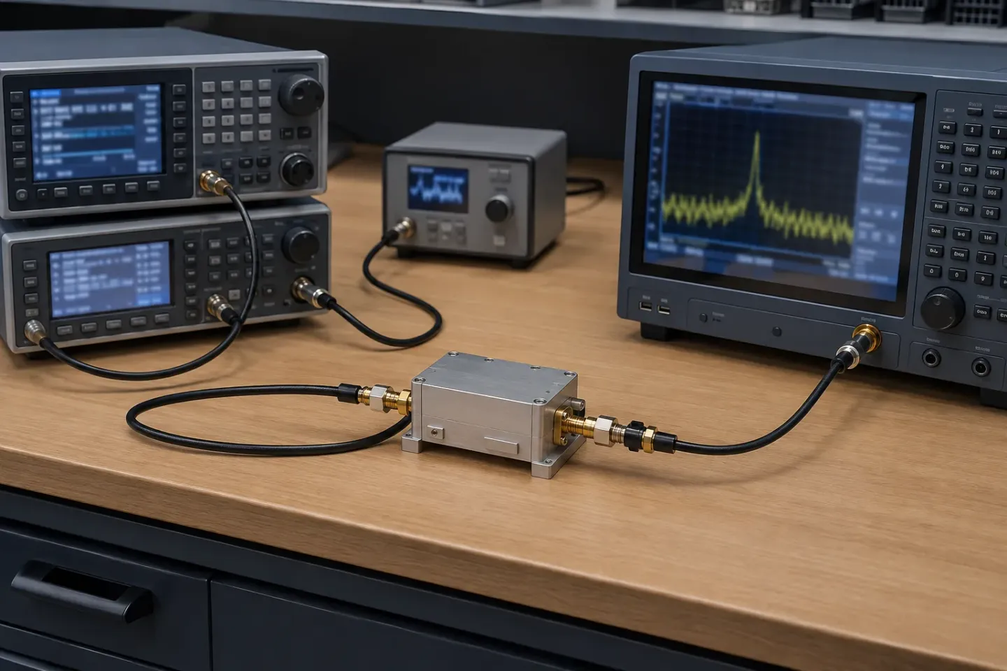
Designing a microwave or millimeter-wave RF module transmitter and receiver—frequently packaged as an integrated transmit/receive (T/R) assembly or RF transceiver module—requires balancing two conflicting cascade equations to prevent sensitivity loss and mixer overload across the receive and transmit chains. On the receive side, the Friis cascaded noise factor equation demands high gain and minimal insertion loss in the first Low-Noise Amplifier (LNA) to mask the high noise figure (25–32 dB) of downstream intermediate-frequency (IF) stages and analog-to-digital converters (ADCs). Simultaneously, the cascaded third-order intercept (IIP3) equation penalizes excessive pre-mixer gain by driving the downconversion mixer into third-order intermodulation distortion (IMD3), collapsing Spurious-Free Dynamic Range (SFDR). On the transmit side, an RF transmitter and receiver assembly must suppress mixer m·f_LO ± n·f_IF spurious products and Local Oscillator (LO) feedthrough before the power amplifier (PA), while trading output power back-off (OBO) against Power-Added Efficiency (PAE) and Adjacent Channel Power Ratio (ACPR).
An RF module transmitter and receiver partitions gain, filtering, and frequency translation across a low-noise receive downconverter (RF → IF/Baseband → ADC) and a high-linearity transmit upconverter (DAC → IF/Baseband → RF → PA). In a 5-stage X-band (10.0 GHz) superheterodyne receiver built around an HMC8410 LNA (1.1 dB NF, +19.5 dB gain, +33 dBm OIP3), an ADRF5720 digital step attenuator (2.0 dB IL, +50 dBm IIP3), and an HMC553ALC3B double-balanced mixer (7.0 dB conversion loss, +18 dBm IIP3), a single LNA achieves NF_total = 4.06 dB, IIP3_total = +3.21 dBm, and a 10 MHz two-tone SFDR = 68.77 dB (MDS = -89.94 dBm). Cascading a second HMC8410 LNA (+39.0 dB LNA gain) improves NF_total by only 0.90 dB (3.16 dB) while collapsing mixer-limited IIP3_total by 19.49 dB to -16.28 dBm (SFDR = 56.37 dB), whereas engaging 12.0 dB of ADRF5720 post-LNA attenuation in high-blocker environments raises IIP3_total to +12.44 dBm and boosts SFDR to 70.86 dB.
This cascade architecture reference resides in the RF and microwave components hub and bridges individual MMIC building blocks to the system-level RF signal chain framework. For shared-antenna duplexing ahead of the first LNA (RP1 to RP3), pair this cascade analysis with RF transceiver module TDD vs. FDD front-end isolation. To extend the transmit EIRP and receive kTB + NF cascade across free-space path loss (FSPL) and X/Ku/Ka-band atmospheric rain attenuation, see our RF link budget calculator and fade margin guide. For directional conversion planning and mixer spur addresses, see upconverter vs. downconverter, frequency converters, and RF, IF, and LO frequency planning.
| Architectural Dimension | Superheterodyne T/R Module (Single / Dual IF) |
Direct-Conversion (Zero-IF / Homodyne Module) |
Direct RF-Sampling Transceiver Module |
|---|---|---|---|
| Representative Hardware & Frequency Span | ADI HMC8410 LNA + ADRF5720 DSA + HMC553ALC3B Mixer + HMC7149 / ADPA7007 PA (6–44 GHz) |
Analog Devices ADRV9009 (75 MHz–6 GHz, 200 MHz RX/TX BW, 450 MHz ORx DPD feedback) + external LNA/PA |
Texas Instruments AFE7950 4T4R2F (5 MHz–12 GHz direct RF ADC/DAC, up to 1.2 GHz IBW) + external LNA/PA |
| Frequency Translation & Channel Filtering | Translates f_RF to intermediate frequency f_IF (70 MHz–2.5 GHz); high-Q SAW/cavity IF filter strips out-of-band blockers before IF gain and ADC |
Translates f_RF directly to baseband quadrature I/Q (f_IF = 0 Hz, f_LO = f_RF); channel selection via active analog baseband LPF + digital FIR |
Digitizes and synthesizes S-, C-, and X-band RF directly with multi-GSPS ADCs/DACs and digital NCOs/DDCs; no analog IF mixers |
| Dominant Spurious & Image Vulnerability | Heterodyne image at f_img = f_RF ± 2·f_IF (requires 60–80 dB pre-mixer image BPF) + m·f_LO ± n·f_RF mixer crossover spurs |
LO self-mixing time-varying DC offsets, even-order distortion (IIP2) demodulating AM blockers to DC, and I/Q gain/phase imbalance |
Nyquist-zone aliasing (requires steep anti-aliasing BPF per Nyquist zone) + track-and-hold HD2/HD3 folding into passband |
| LO Phase Noise & Clock Jitter Bottleneck | LO phase noise L(Δf) mixes reciprocally with adjacent blockers (N_recip = P_blk + L(Δf) + 10·log10(BW)); mitigated by YIG oscillators |
Internal fractional-N PLL/VCO phase noise and quadrature phase error (Δφ) bound high-order 256-QAM Error Vector Magnitude (EVM) |
Sampling clock aperture jitter t_j caps high-RF SNR via SNR_jitter = -20·log10(2·π·f_RF·t_j) (67.1 dB at 10 GHz, t_j = 70 fs) |
| Transmit Spur Control & Linearization | Post-mixer RF bandpass filter rejects f_LO feedthrough (-11 dBc unfiltered) and f_LO ± f_IF unused sideband by >= 50 dB ahead of GaN PA |
Active DSP quadrature error correction (QEC), LO carrier leakage nulling (<= -60 dBc), and 450 MHz ORx closed-loop Digital Predistortion (DPD) |
Direct RF DAC synthesis + reconstruction BPF stripping f_s ± f_RF sampling images + dual feedback (2F) paths for wideband PA DPD |
Superheterodyne vs. Direct-Conversion (Zero-IF) vs. Direct-RF Sampling T/R Module Architectures
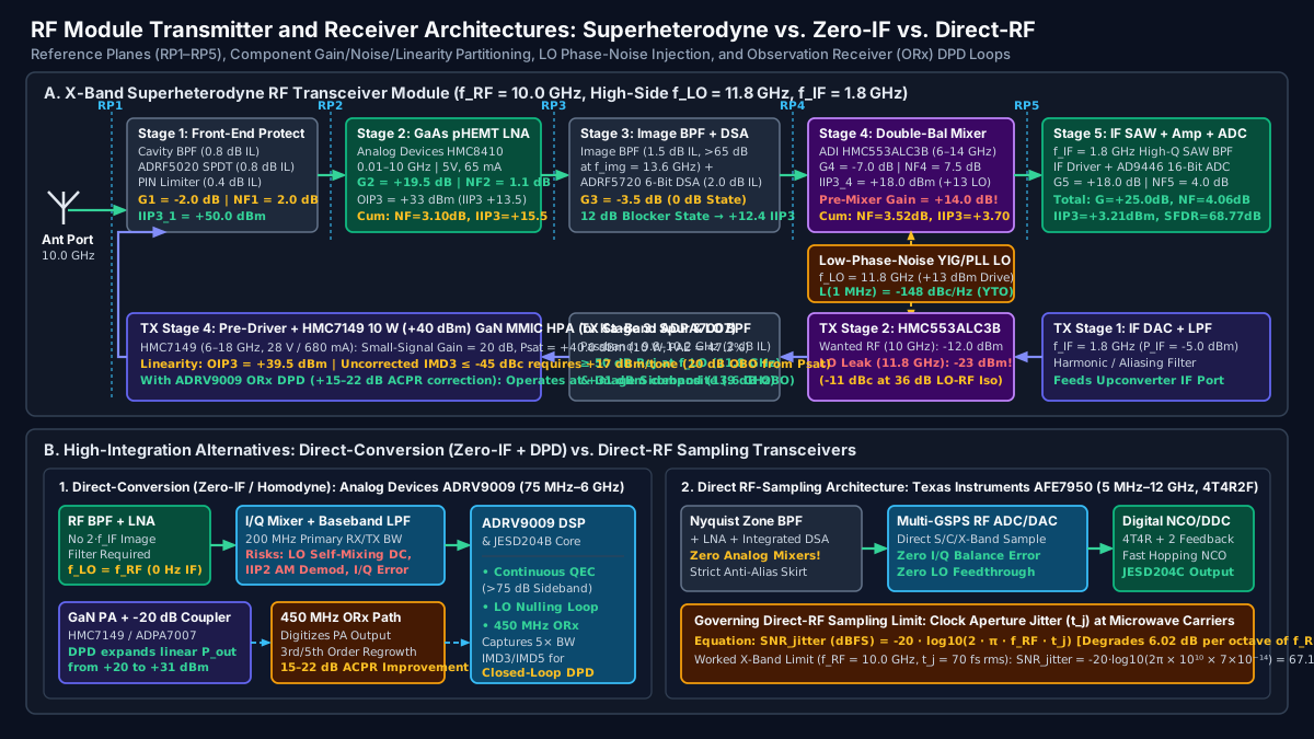
Selecting the internal topology of an RF module transmitter and receiver determines how physical filtering and digital calibration are partitioned between the antenna port (RP1) and the data converter interface (RP5). Across modern radar RF components, satellite ground terminals, electronic warfare (EW) receivers, and wideband tactical datalinks, engineers choose among three primary RF transceiver module architectures—or combine them in hybrid dual-stage assemblies.
1. Superheterodyne T/R Modules (Single or Dual IF)
In a superheterodyne RF transmitter and receiver, a low-noise Local Oscillator (f_LO) and fundamental double-balanced mixer such as the Analog Devices HMC553ALC3B (6 GHz to 14 GHz passive GaAs MMIC mixer) translate the microwave carrier f_RF (10.0 GHz in Panel A) to a fixed intermediate frequency f_IF (1.8 GHz with high-side f_LO = 11.8 GHz, where f_IF = |f_LO - f_RF|).
Moving the signal to a fixed IF enables two physical advantages that neither Zero-IF nor Direct-RF sampling can replicate at X-, Ku-, or Ka-band:
- Hardware blocker protection ahead of high-gain IF stages: High-Q surface acoustic wave (SAW), ceramic, or cavity bandpass filters at
f_IFexhibit steep shape factors that strip strong adjacent-channel interferers (+10 to +20 dBabove the desired signal) before the final IF variable-gain amplifier (VGA) and ADC driver (Stage 5). - Freedom from DC offset and flicker (
1/f) noise: Becausef_IFsits hundreds of megahertz or gigahertz above0 Hz, AC-coupled IF amplifiers completely block mixer LO self-mixing DC offsets and semiconductor1/fcorner noise.
The price of superheterodyne conversion is the image frequency at f_img = f_RF + 2·f_IF (for high-side injection, 10.0 GHz + 2 × 1.8 GHz = 13.6 GHz) or f_RF - 2·f_IF (for low-side injection). Any noise or interference at f_img mixes with f_LO to land directly inside the wanted 1.8 GHz IF passband. Consequently, Stage 1 (preselector) and Stage 3 (interstage image-reject filter) must provide 60 to 80 dB of hardware rejection at f_img prior to RP4.
2. Direct-Conversion (Zero-IF / Homodyne) Transceiver Modules (ADRV9009)
A Direct-Conversion (Zero-IF) RF transceiver module sets the Local Oscillator equal to the carrier frequency (f_LO = f_RF, so f_IF = 0 Hz) and splits the receive and transmit paths into in-phase (I, 0°) and quadrature (Q, 90°) baseband channels. The Analog Devices ADRV9009 (75 MHz to 6 GHz dual transceiver) exemplifies this architecture: it integrates dual 200 MHz receive chains, dual 200 MHz transmit synthesis chains (450 MHz total synthesis BW), fractional-N PLL synthesizers, and a dedicated 450 MHz Observation Receiver (ORx) on a single monolithic die.
By setting f_IF = 0 Hz, the 2 × f_IF heterodyne image collapses onto the desired channel itself, where it is suppressed by quadrature phase cancellation rather than bulky microwave cavity filters. However, Zero-IF modules introduce three impairments that must be continuously calibrated:
- Quadrature Gain (
ΔA) and Phase (Δφ) Imbalance: Finite amplitude and phase mismatch between theIandQbranches leaks energy from the negative-frequency half of the channel (-f_BB) into the positive-frequency half (+f_BB). The resulting Image Rejection Ratio (IRR) is governed by:
IRR (dB) = -10 × log10( [ 1 - 2 × (1 + ΔA) × cos(Δφ) + (1 + ΔA)^2 ] / [ 1 + 2 × (1 + ΔA) × cos(Δφ) + (1 + ΔA)^2 ] ) ≈ -10 × log10( (ΔA^2 + Δφ_rad^2) / 4 )
An uncalibrated 0.5 dB (5.9%) gain error and 3.0° (0.0524 rad) phase error limit IRR to just 28.1 dB; the ADRV9009 runs continuous background Quadrature Error Correction (QEC) tracking algorithms to push sideband and image suppression beyond 75 dB.
2. LO Self-Mixing DC Offset: Finite LO-to-RF isolation allows f_LO energy to leak onto the LNA/mixer RF path, reflect off the preselector or antenna impedance, and mix with itself (f_LO - f_LO = 0 Hz), creating a large, time-varying DC offset at the baseband ADC input.
3. Even-Order Nonlinearity (IIP2): Any strong amplitude-modulated (AM/QAM/OFDM) blocker experiences second-order distortion in the quadrature mixer, demodulating its low-frequency envelope directly onto DC baseband.
3. Direct RF-Sampling Transceiver Modules (TI AFE7950) and Clock Aperture Jitter
At frequencies up to X-band (12 GHz), multi-gigasample data converters eliminate analog mixers altogether. The Texas Instruments AFE7950 (5 MHz to 12 GHz, 4T4R2F direct RF-sampling transceiver) integrates four RF transmit DACs, four RF receive ADCs, two feedback (2F) paths, integrated digital step attenuators (DSAs), and numerically controlled oscillators (NCOs) in a single module core.
While Direct-RF sampling removes I/Q quadrature imbalance and analog LO feedthrough, its high-frequency dynamic range is bounded by sampling clock aperture jitter (t_j, rms seconds). When an RF ADC samples a high-frequency sinusoid f_RF, timing uncertainty t_j on the sampling clock edges translates phase noise directly into voltage error, bounding the maximum achievable Signal-to-Noise Ratio (SNR_jitter) per Analog Devices MT-003:
SNR_jitter (dBFS) = -20 × log10( 2 × π × f_RF × t_j )
Notice the 20 × log10(f_RF) penalty: every doubling (octave) of the RF carrier frequency degrades jitter-limited ADC SNR by 6.02 dB. Evaluating a state-of-the-art sampling clock with rms aperture jitter t_j = 70 fs (7.0 × 10^-14 s):
- At
f_RF = 1.0 GHz(L-band):SNR_jitter = -20 × log10(2 × π × 10^9 × 7.0 × 10^-14) = -20 × log10(4.398 × 10^-4) =67.13 dB. - At
f_RF = 10.0 GHz(X-band):SNR_jitter = -20 × log10(2 × π × 10^10 × 7.0 × 10^-14) = -20 × log10(4.398 × 10^-3) =47.13 dB.
Because a 47.13 dB broadband jitter floor over a multi-gigahertz Nyquist zone degrades sensitivity under strong blockers, high-SFDR X-, Ku-, and Ka-band (8–40 GHz) RF module transmitter and receiver designs frequently use a hybrid dual-stage architecture: a microwave superheterodyne block converter translates 8–40 GHz down to a 1.0–3.0 GHz IF, where an ADRV9009 or AFE7950 digitizes the IF and executes closed-loop PA Digital Predistortion (DPD).
Takeaway: Choose superheterodyne conversion when high-Q IF filtering and low-phase-noise YIG/DRO local oscillators are required to preserve > 68 dB SFDR at microwave frequencies; use Zero-IF (ADRV9009) or Direct-RF (AFE7950) below 6–12 GHz or as the programmable IF/baseband engine behind a microwave block converter.
Receive (RX) Chain Cascade Analysis: Friis Noise Factor (F_total) vs. Cascaded Linearity (IIP3_total)
Every receive chain inside an RF module transmitter and receiver must simultaneously amplify microvolt-level antenna signals above the data converter’s thermal and quantization noise floor while preventing milliwatt-level interferers from generating in-band third-order intermodulation products. As derived in Analog Devices Tutorial MT-006 (ADC Noise Figure — An Often Misunderstood and Misinterpreted Specification) and Michael Steer’s Microwave and RF Design IV: Modules, Chapter 7 (Cascade of Modules), noise and distortion propagate through a k-stage cascade via opposite mathematical weightings of cumulative power gain.
1. Exact Friis Cascaded Noise Factor Equation (F_total) and ADC Noise Suppression
For a cascade of k two-port stages where Stage i has linear available power gain G_i = 10^(G_i_dB / 10) and linear noise factor F_i = 10^(NF_i_dB / 10) (referenced to standard thermal temperature T_0 = 290 K, where k_B × T_0 = 4.00 × 10^-21 W/Hz = -174.0 dBm/Hz), the total input-referred Friis noise factor (F_total) and Cascaded Noise Figure (NF_total) are:
F_total = F_1 + (F_2 - 1) / G_1 + (F_3 - 1) / (G_1 × G_2) + (F_4 - 1) / (G_1 × G_2 × G_3) + ... + (F_k - 1) / (G_1 × G_2 × ... × G_{k-1})
NF_total (dB) = 10 × log10(F_total)
Three design rules follow immediately from the Friis equation:
- Passive loss ahead of the first LNA (
Stage 1) adds dB-for-dB toNF_total: For any passive reciprocal filter, switch, or limiter operating atT_0 = 290 Kwith insertion lossL_1(dB, linear loss ratioL_1_lin = 10^(L_1_dB / 10)), the linear power gain isG_1 = 1 / L_1_linand the linear noise factor isF_1 = L_1_lin. SubstitutingF_1 = L_1_linandG_1 = 1 / L_1_lininto the first two terms of the Friis equation gives:
F_12 = L_1_lin + (F_2 - 1) / (1 / L_1_lin) = L_1_lin × F_2 ⇒ NF_12 (dB) = L_1 (dB) + NF_2 (dB)
In our X-band front end (Stage 1), the cavity preselector (0.8 dB IL), ADRF5020 silicon SPDT switch (0.8 dB IL at 10 GHz), and PIN cleanup limiter (0.4 dB IL) contribute L_1 = 2.0 dB of passive insertion loss (G_1 = -2.0 dB = 0.6310, F_1 = 1.5849). Followed by the Analog Devices HMC8410 (0.01–10 GHz GaAs pHEMT LNA with NF_2 = 1.1 dB, G_2 = +19.5 dB), the cumulative noise figure at RP3 (NF_12) is 2.0 dB + 1.1 dB = 3.10 dB (F_12 = 2.0417).
2. High LNA gain suppresses passive mixer loss (Stage 4): The HMC553ALC3B double-balanced mixer has 7.0 dB conversion loss (G_4 = -7.0 dB = 0.1995) and NF_4 = 7.5 dB (F_4 = 5.6234), preceded by Stage 3 (1.5 dB image BPF + 2.0 dB ADRF5720 DSA insertion loss, G_3 = -3.5 dB = 0.4467, F_3 = 2.2387). Because the net pre-mixer gain G_1 × G_2 × G_3 = +14.0 dB (25.1189 linear) sits in the denominator (F_4 - 1) / (G_1 × G_2 × G_3) = 4.6234 / 25.1189 = 0.1841, the mixer raises the system noise figure by only 0.37 dB (from 3.15 dB to 3.52 dB).
3. Why RF/IF gain is mandatory ahead of the ADC: As proven in Analog Devices MT-006, a high-speed data converter’s effective noise figure (NF_ADC) is governed by its full-scale input power P_FS (dBm), signal-to-noise ratio SNR_ADC (dB), and Nyquist/filtered noise bandwidth BW (Hz):
NF_ADC (dB) = P_FS (dBm) + 174.0 dBm/Hz - SNR_ADC (dB) - 10 × log10(BW_Hz)
For the 16-bit, 80/100 MSPS AD9446 ADC analyzed in MT-006 (P_FS = +4.0 dBm for 2 V p-p across a 200 Ω load transformation, SNR = 80.0 dB, and BW = 40 MHz), NF_ADC = +4.0 + 174.0 - 80.0 - 76.02 = 30.1 dB (F_ADC = 1023.3). Preceding the ADC with an IF buffer amplifier (G_IF = +18.0 dB, NF = 3.5 dB) yields a composite Stage 5 subsystem noise figure of NF_5 = 4.0 dB (F_5 = 2.5119), keeping total receiver noise figure at NF_total = 4.06 dB (F_total = 2.5446).
2. Exact Cascaded Third-Order Intercept Equation (IIP3_total)
When two closely spaced interfering tones at f_1 and f_2 (|f_1 - f_2| = Δf) enter a nonlinear cascade, third-order intermodulation distortion (IMD3) products appear at 2·f_1 - f_2 and 2·f_2 - f_1—directly inside the passband alongside the desired signal. As derived in Steer, Chapter 7, for k stages where Stage i has input third-order intercept power IIP3_i (mW, where IIP3_i_mW = 10^(IIP3_i_dBm / 10)) and output intercept OIP3_i_dBm = IIP3_i_dBm + G_i_dB, the cascaded input third-order intercept (IIP3_total) under uncorrelated (power-summed) intermodulation products is:
1 / IIP3_total (mW^-1) = 1 / IIP3_1 + G_1 / IIP3_2 + (G_1 × G_2) / IIP3_3 + (G_1 × G_2 × G_3) / IIP3_4 + ... + (G_1 × G_2 × ... × G_{k-1}) / IIP3_k
IIP3_total (dBm) = 10 × log10( IIP3_total_mW )
(Note: When stage intermodulation products add coherently in phase, replace each power ratio term (G_1...G_{i-1})/IIP3_i with its square root and square the sum at the end, yielding a ~2 to 3 dB more conservative lower bound.)
Compare the denominator of the Friis equation against the numerator of the cascaded IIP3 equation:
- In Friis (
F_total), cumulative gainG_1 × G_2 × ... × G_{i-1}sits in the denominator, dividing down the noise of later stages. - In Linearity (
1 / IIP3_total), cumulative gainG_1 × G_2 × ... × G_{i-1}sits in the numerator, multiplying up the nonlinearity of later stages!
In our baseline X-band receiver (State A), examine each stage’s input-referred intercept contribution (G_1...G_{i-1}) / IIP3_i:
- Stage 1 (
Preselector + ADRF5020 + Limiter,IIP3_1 = +50.0 dBm = 100,000 mW):1 / IIP3_1 = 1.00 × 10^-5 mW^-1(negligible). - Stage 2 (
HMC8410 LNA,OIP3_2 = +33.0 dBm,G_2 = +19.5 dB→IIP3_2 = +13.5 dBm = 22.387 mW): Referred toRP1throughG_1 = -2.0 dB(0.6310), its effective input intercept is+13.5 dBm - (-2.0 dB) = +15.50 dBm(G_1 / IIP3_2 = 0.02818 mW^-1). - Stage 3 (
Image BPF + ADRF5720 DSA at 0 dB,IIP3_3 = +50.0 dBm = 100,000 mW): Referred toRP1throughG_1 × G_2 = +17.5 dB(56.234), its contribution is56.234 / 100,000 = 0.00056 mW^-1(+32.5 dBmequivalent). - Stage 4 (
HMC553ALC3B Mixer,IIP3_4 = +18.0 dBm = 63.096 mW): Referred toRP1throughG_1 × G_2 × G_3 = +14.0 dB(25.1189), its effective input intercept is+18.0 dBm - 14.0 dB = +4.00 dBm(25.1189 / 63.096 = 0.39811 mW^-1—83.4%of the entire receiver’s distortion budget!). - Stage 5 (
IF Amp + SAW + AD9446,IIP3_5 = +20.0 dBm = 100.0 mW): Referred toRP1throughG_1 × G_2 × G_3 × G_4 = +7.0 dB(5.0119), its effective input intercept is+20.0 dBm - 7.0 dB = +13.00 dBm(5.0119 / 100.0 = 0.05012 mW^-1).
Summing all five terms yields 1 / IIP3_total = 0.47698 mW^-1, so IIP3_total = 2.0965 mW = +3.21 dBm (and output intercept OIP3_total = +3.21 dBm + 25.0 dB = +28.21 dBm).
3. Complete 5-Stage Worked X-Band Superheterodyne RX Cascade Budget (State A)
The table below documents every stage and cumulative metric across the 10.0 GHz superheterodyne receive chain for an instantaneous IF detection bandwidth of BW = 10 MHz (10 × log10(10^7 Hz) = 70.0 dB-Hz) and a required detection threshold of SNR_min = 10.0 dB:
| Stage & Reference Plane | Hardware Component & Operating Bias | Stage Gain (G_i) |
Stage NF (NF_i) |
Stage IIP3_i (OIP3_i) |
Cumulative Gain (G_cum) |
Cumulative Friis NF_cum |
Cumulative IIP3_cum (OIP3_cum) |
10 MHz Noise Floor (MDS at 10 dB SNR) |
10 MHz Two-Tone SFDR |
|---|---|---|---|---|---|---|---|---|---|
Stage 1 (RP1 → RP2): Preselector + Switch + Limiter |
Cavity BPF (0.8 dB) + ADRF5020 (0.8 dB) + PIN Limiter (0.4 dB) |
-2.0 dB (0.631×) |
2.00 dB (F_1 = 1.585) |
+50.0 dBm (+48.0 dBm) |
-2.0 dB |
2.00 dB (F = 1.585) |
+50.00 dBm (+48.00 dBm) |
-102.00 dBm (-92.00 dBm) |
101.33 dB |
Stage 2 (RP2 → RP3): GaAs pHEMT Low-Noise Amplifier |
Analog Devices HMC8410 (0.01–10 GHz, 5 V, 65 mA) |
+19.5 dB (89.13×) |
1.10 dB (F_2 = 1.288) |
+13.5 dBm (+33.0 dBm) |
+17.5 dB |
3.10 dB (F = 2.042) |
+15.50 dBm (+33.00 dBm) |
-100.90 dBm (-90.90 dBm) |
77.60 dB |
Stage 3 (RP3 → RP4): Image BPF + 6-Bit Silicon DSA |
Image BPF (1.5 dB IL) + ADRF5720 DSA (0 dB state, 2.0 dB IL) |
-3.5 dB (0.447×) |
3.50 dB (F_3 = 2.239) |
+50.0 dBm (+46.5 dBm) |
+14.0 dB |
3.15 dB (F = 2.066) |
+15.41 dBm (+29.41 dBm) |
-100.85 dBm (-90.85 dBm) |
77.51 dB |
Stage 4 (RP4 → RP5): Double-Balanced Mixer |
Analog Devices HMC553ALC3B (6–14 GHz, +13 dBm LO drive) |
-7.0 dB (0.200×) |
7.50 dB (F_4 = 5.623) |
+18.0 dBm (+11.0 dBm) |
+7.0 dB |
3.52 dB (F = 2.250) |
+3.70 dBm (+10.70 dBm) |
-100.48 dBm (-90.48 dBm) |
69.45 dB |
Stage 5 (RP5 → ADC): IF SAW + Buffer + Digitizer |
1.8 GHz SAW BPF + IF Driver + AD9446 16-bit ADC (MT-006) |
+18.0 dB (63.10×) |
4.00 dB (F_5 = 2.512) |
+20.0 dBm (+38.0 dBm) |
+25.0 dB |
4.06 dB (F = 2.545) |
+3.21 dBm (+28.21 dBm) |
-99.94 dBm (-89.94 dBm) |
68.77 dB |
4. Four-State Dynamic Range Comparison: Dual-LNA Overdrive (State B) vs. 12 dB DSA Blocker Mode (State C)
What happens when an engineer alters the pre-mixer gain distribution or widens the instantaneous channel bandwidth? Comparing four operating states of the exact same hardware chain reveals the fundamental trade-off of RF module transmitter and receiver design:
| Operating Mode & Gain Configuration | Net Gain (G_total) |
Cascaded Friis NF_total |
Integrated Noise Floor (N_0) |
Minimum Detectable Signal (MDS, 10 dB SNR) |
Cascaded IIP3_total |
Two-Tone SFDR |
Dominant Bottleneck & Engineering Consequence |
|---|---|---|---|---|---|---|---|
State A: Baseline Single-LNA Mode (1× HMC8410 +19.5 dB, ADRF5720 DSA = 0 dB, BW = 10 MHz) |
+25.0 dB |
4.06 dB |
-99.94 dBm |
-89.94 dBm |
+3.21 dBm |
68.77 dB |
Balanced cascade: HMC553ALC3B mixer (+14 dB pre-mixer gain) sets IIP3, while Stage 1 loss (2.0 dB) + HMC8410 (1.1 dB) set NF. |
State B: Dual-LNA Overdrive Mode (2× Cascaded HMC8410 +39.0 dB, DSA = 0 dB, BW = 10 MHz) |
+44.5 dB |
3.16 dB (-0.90 dB vs. A) |
-100.84 dBm |
-90.84 dBm |
-16.28 dBm (-19.49 dB collapse!) |
56.37 dB (-12.40 dB loss!) |
Severe mixer overload: +33.5 dB (2239×) pre-mixer gain overwhelms the +18 dBm mixer; 0.90 dB better NF costs 12.40 dB of SFDR! |
State C: High-Blocker Linearity Mode (1× HMC8410, ADRF5720 DSA = 12.0 dB Atten, BW = 10 MHz) |
+13.0 dB |
10.15 dB (+6.09 dB vs. A) |
-93.85 dBm |
-83.85 dBm |
+12.44 dBm (+9.23 dB boost!) |
70.86 dB (+2.09 dB net gain!) |
Blocker shield: 12 dB post-LNA attenuation drops pre-mixer gain to +2.0 dB, shielding the mixer so IIP3 approaches the HMC8410 LNA ceiling (+15.5 dBm). |
State D: Wideband 100 MHz Channel Mode (1× HMC8410, DSA = 0 dB, BW = 100 MHz) |
+25.0 dB |
4.06 dB |
-89.94 dBm (+10.0 dB vs. A) |
-79.94 dBm |
+3.21 dBm |
62.10 dB (-6.67 dB vs. A) |
Thermal bandwidth expansion: 10× wider bandwidth raises N_0 by +10.0 dB and compresses two-tone SFDR by (2/3) × 10 dB = 6.67 dB. |
Look closely at State B versus State C:
- Placing two HMC8410 LNAs in series (
State B) is a common design error when attempting to squeeze out an extra fraction of a decibel of noise figure. Because the first LNA already provides+19.5 dBof gain, the second LNA trimsNF_totalby only0.90 dB(4.06 dB → 3.16 dB), yet it multiplies the power entering the HMC553ALC3B mixer by89.13×(+19.5 dB). CascadedIIP3_totalplunges from+3.21 dBmto-16.28 dBm, slashingSFDRfrom68.77 dBdown to56.37 dB. - Conversely, placing the 6-bit ADRF5720 silicon digital step attenuator (
0.5 dBLSB,31.5 dBrange,+50 dBmIIP3) after the first LNA (Stage 3) gives the receiver an adaptive linearity control knob. When strong in-band blockers appear, stepping theADRF5720to12.0 dBattenuation (State C, totalStage 3loss =1.5 + 2.0 + 12.0 = 15.5 dB, reducing net pre-mixer gain from+14.0 dBto+2.0 dB) elevates cascadedIIP3_totalby+9.23 dB(to+12.44 dBm) and increases two-toneSFDRto70.86 dB.
Takeaway: Size pre-mixer LNA gain so the downconversion mixer degrades cascade noise figure by 0.4 to 1.0 dB (G_pre-mixer ≈ 12 to 16 dB), and place a high-IIP3 digital step attenuator (ADRF5720) between the LNA and mixer to trade noise figure for +9 to +12 dB higher IIP3 under heavy interference.
Spurious-Free Dynamic Range (SFDR) and Local Oscillator Reciprocal Mixing (RMDR)
While NF_total defines the lower sensitivity boundary of an RF module transmitter and receiver and IIP3_total defines its upper third-order distortion ceiling, system architects combine both metrics into a single figure of merit: Two-Tone Spurious-Free Dynamic Range (SFDR)—and then audit whether Local Oscillator phase noise (L(Δf)) undercuts that dynamic range via Reciprocal Mixing (RMDR).
1. Deriving Two-Tone Third-Order SFDR (10 MHz vs. 100 MHz Bandwidth)
As formulated in Michael Steer’s Microwave and RF Design IV: Modules, Chapter 4 (Noise, Distortion, and Dynamic Range) and Analog Devices MT-003, for two equal-power input tones of power P_in (dBm per tone), the input-referred power of each third-order intermodulation tone (2·f_1 - f_2 and 2·f_2 - f_1) rises at a 3:1 logarithmic slope:
P_IMD3_in (dBm) = 3 × P_in - 2 × IIP3_total
The maximum tone input power P_in_max_SFDR before P_IMD3_in emerges above the receiver’s integrated input-referred thermal noise floor N_0 (N_0 = -174.0 dBm/Hz + 10·log10(BW_Hz) + NF_total) occurs when 3 × P_in_max_SFDR - 2 × IIP3_total = N_0. Subtracting N_0 from P_in_max_SFDR yields the governing Two-Tone Third-Order SFDR Equation:
SFDR (dB) = P_in_max_SFDR - N_0 = (2 / 3) × ( IIP3_total - N_0 )
SFDR (dB) = (2 / 3) × [ IIP3_total (dBm) - ( -174.0 dBm/Hz + 10 × log10(BW_Hz) + NF_total (dB) ) ]
(Note: When MDS = N_0 + SNR_min is used as the lower sensitivity threshold for modulation schemes requiring SNR_min (dB), the operational dynamic range above MDS is DR_op = SFDR - SNR_min.)
Evaluating our baseline X-band receiver (State A: NF_total = 4.06 dB, IIP3_total = +3.21 dBm) across 10 MHz versus 100 MHz instantaneous bandwidths:
- At
BW = 10 MHz(10·log10(10^7) = 70.0 dB-Hz):- Input thermal noise floor:
N_0 = -174.0 + 70.0 + 4.06 =-99.94 dBm. - Minimum Detectable Signal (
SNR_min = 10 dB):MDS = -99.94 + 10.0 =-89.94 dBm. - Maximum spur-free tone level:
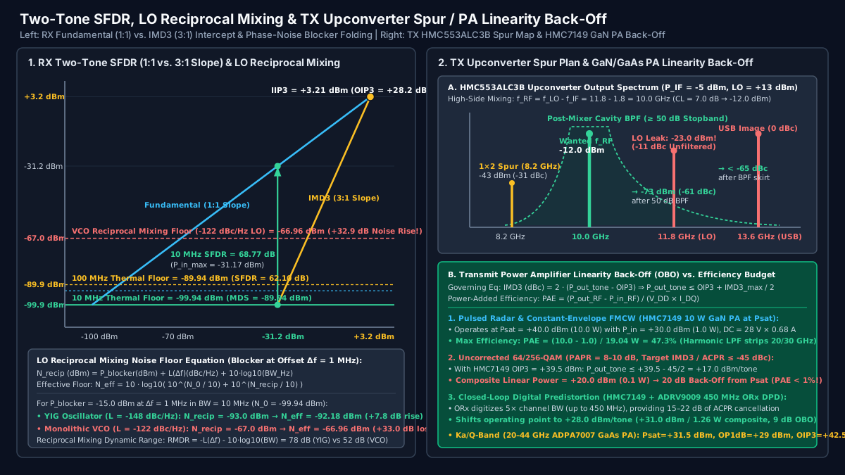
P_in_max_SFDR = -99.94 + (2/3) × (3.21 - (-99.94)) = -99.94 + 68.77 =-31.17 dBm. - Two-Tone
SFDR(10 MHz):(2/3) × (3.21 - (-99.94)) =68.77 dB.
- Input thermal noise floor:
- At
BW = 100 MHz(State D,10·log10(10^8) = 80.0 dB-Hz):- Input thermal noise floor:
N_0 = -174.0 + 80.0 + 4.06 =-89.94 dBm(MDS = -79.94 dBm). - Two-Tone
SFDR(100 MHz):(2/3) × (3.21 - (-89.94)) =62.10 dB(a6.67 dBcompression for every10×expansion in channel bandwidth).
- Input thermal noise floor:
2. Local Oscillator Phase Noise (L(Δf)) and Reciprocal Mixing Dynamic Range (RMDR)
In real electromagnetic environments, a receiver’s usable dynamic range is frequently limited not by IIP3_total, but by Local Oscillator Reciprocal Mixing. Suppose a weak desired signal at f_RF = 10.000 GHz arrives alongside a strong single-tone off-channel blocker of power P_blocker (dBm) at frequency offset Δf = 1.0 MHz (f_blocker = 10.001 GHz). Even if P_blocker = -15.0 dBm sits 18.21 dB below IIP3_total = +3.21 dBm—and even if the post-mixer 1.8 GHz IF SAW filter completely rejects the downconverted blocker at 1.801 GHz—the Local Oscillator (f_LO = 11.800 GHz) possesses a phase noise sideband L(Δf) (dBc/Hz) at offset Δf = 1.0 MHz.
Inside the HMC553ALC3B mixer, the blocker at 10.001 GHz mixes with the LO phase-noise energy at 11.801 GHz (f_LO + Δf) to translate broadband phase noise directly to 11.801 GHz - 10.001 GHz = 1.800 GHz—right on top of the wanted IF passband! The input-referred reciprocal mixing noise power N_recip (dBm) integrated across channel bandwidth BW (Hz) and the resulting Reciprocal Mixing Dynamic Range (RMDR) are:
N_recip (dBm) = P_blocker (dBm) + L(Δf) (dBc/Hz) + 10 × log10(BW_Hz)
N_eff (dBm) = 10 × log10( 10^(N_0 / 10) + 10^(N_recip / 10) )
RMDR (dB) = P_blocker - N_recip = -L(Δf) (dBc/Hz) - 10 × log10(BW_Hz)
Compare two 11.8 GHz Local Oscillator sources driving our State A receiver (BW = 10 MHz, N_0 = -99.94 dBm) in the presence of a P_blocker = -15.0 dBm interferer at Δf = 1.0 MHz offset:
Local Oscillator Source Candidate (f_LO = 11.8 GHz) |
SSB Phase Noise L(1 MHz) |
Reciprocal Mixing Noise (N_recip in 10 MHz) |
Composite Receiver Noise Floor (N_eff) |
Desensitization (Noise Floor Rise) |
Reciprocal Mixing Dynamic Range (RMDR) |
|---|---|---|---|---|---|
| Candidate 1: Wideband Monolithic SiGe/GaAs VCO PLL | -122.0 dBc/Hz |
-15.0 - 122.0 + 70.0 = -67.00 dBm |
-66.96 dBm |
+32.98 dB sensitivity collapse! |
52.00 dB (Blocker-limited; wastes 16.8 dB of mixer SFDR) |
| Candidate 2: Low-Noise YIG-Tuned Oscillator (YTO) | -148.0 dBc/Hz |
-15.0 - 148.0 + 70.0 = -93.00 dBm |
-92.18 dBm |
+7.76 dB (25.2 dB cleaner than VCO) |
78.00 dB (Exceeds 68.77 dB two-tone SFDR by +9.2 dB) |
As the calculation demonstrates, pairing a high-linearity mixer with a noisy -122 dBc/Hz monolithic VCO causes a single -15 dBm blocker 1 MHz away to elevate the receiver noise floor by 32.98 dB (from -99.94 dBm to -66.96 dBm), rendering the 68.77 dB two-tone SFDR meaningless. Specifying a high-Q YIG-tuned oscillator with L(1 MHz) = -148 dBc/Hz pushes RMDR to 78.00 dB, preserving mixer-limited dynamic range.
Takeaway: Always verify that Local Oscillator phase noise satisfies L(Δf) <= N_0 - P_blocker_max - 10·log10(BW) at the closest expected blocker offset Δf; otherwise, reciprocal mixing degrades receiver sensitivity long before the mixer reaches its IIP3 limit.
Transmit (TX) Chain Architecture: Upconverter Spur Filtering, LO Feedthrough, and GaN/GaAs PA Back-Off
In the transmit half of an RF module transmitter and receiver, the engineering priorities invert: instead of protecting a sensitive ADC from noise and overload, the transmit cascade must synthesize a spectrally pure microwave waveform and amplify it to watt- or ten-watt levels without violating out-of-band spurious masks, Local Oscillator leakage limits, or Adjacent Channel Power Ratio (ACPR) regulations.
1. Upconverter Mixer Spur Budget (m·f_LO ± n·f_IF) and -11 dBc Unfiltered LO Feedthrough
Consider the X-band superheterodyne transmit path in Figure 1 (Panel A) and Figure 3 (Right Panel), which upconverts a modulated IF carrier at f_IF = 1.8 GHz (P_IF = -5.0 dBm) using a high-side Local Oscillator at f_LO = 11.8 GHz (P_LO = +13.0 dBm) inside an Analog Devices HMC553ALC3B double-balanced mixer (6–14 GHz) to generate the desired lower-sideband RF output at f_RF = f_LO - f_IF = 10.0 GHz.
From the HMC553ALC3B datasheet (Conversion Loss = 7.0 dB, LO-to-RF Isolation = 36 dB typical, LO-to-IF Isolation = 38 dB, IIP3 = +18.0 dBm), four distinct spectral components exit the mixer’s RF port before filtering:
- Desired Lower-Sideband RF Carrier (
f_RF = f_LO - f_IF = 10.0 GHz): Exits atP_RF = P_IF - CL = -5.0 dBm - 7.0 dB =-12.0 dBm(0 dBcreference). - Unfiltered LO Feedthrough (
f_LO = 11.8 GHz): Attenuated only by the double-balanced diode ring’s intrinsic36.0 dBLO-to-RF isolation, the+13.0 dBmLO drive leaks out of the RF port at:
P_LO_leak (dBm) = P_LO (dBm) - Iso_LO_RF (dB) = +13.0 dBm - 36.0 dB = -23.0 dBm
Compared against the -12.0 dBm desired RF carrier, unfiltered LO feedthrough sits at -23.0 - (-12.0) = -11.0 dBc—just 1.8 GHz above the passband! If allowed to enter the +20 dB driver and HMC7149 10 W GaN PA, this -23 dBm LO tone would be amplified to +17 dBm (50 mW) and intermodulate with the main carrier.
3. Unwanted Upper-Sideband Image (f_USB = f_LO + f_IF = 13.6 GHz): Exits a standard double-balanced mixer at equal amplitude to the lower sideband (-12.0 dBm / 0 dBc), sitting 2 × f_IF = 3.6 GHz above the desired carrier.
4. Harmonic Intermodulation Spurs (m·f_LO ± n·f_IF): Even though double-balanced symmetry suppresses even-by-even products, the m = 1, n = 2 product at f_LO - 2·f_IF = 11.8 - 3.6 = 8.2 GHz exits near -43 dBm (-31 dBc), sitting 1.8 GHz below the 10.0 GHz carrier.
To suppress radiated LO leakage and out-of-band spurs below -60 dBc, a post-mixer bandpass filter (TX Stage 3) centered at 10.0 GHz (IL ≈ 2.0 dB) must provide >= 50 dB stopband rejection at 11.8 GHz (f_LO) (pushing -11 dBc LO leakage down to -61 dBc / -73 dBm), >= 60 dB rejection at 13.6 GHz (f_USB), and >= 35 dB rejection at 8.2 GHz (1×2 spur) before the pre-driver and final power amplifier.
2. GaN (HMC7149) vs. Millimeter-Wave GaAs (ADPA7007) Power Amplifier Linearity Back-Off (OBO)
At the output of the RF module transmitter and receiver, the High-Power Amplifier (HPA) dominates DC power consumption, thermal dissipation, and spectral regrowth. Compare two verified MMIC power amplifiers across X/Ku-band and Ka/Q-band:
- Analog Devices HMC7149 (
6 GHz to 18 GHz,10 WGaN MMIC PA): Biased atV_DD = +28 V,I_DQ = 680 mA(P_DC_quiescent = 19.04 W), delivering20.0 dBsmall-signal gain,+40.0 dBm(10.0 W) saturated output power (Psat) with10.0 dBpower gain at saturation, and+39.5 dBmOutput Third-Order Intercept (OIP3) measured at+28 dBm/tone. - Analog Devices ADPA7007 (
20 GHz to 44 GHz,> 1 WGaAs pHEMT MMIC PA): Biased atV_DD = +5 V,I_DQ = 1400 mA(7.0 WDC), delivering20.5 dBsmall-signal gain,+29.0 dBmoutput1 dBcompression (OP1dB),+31.5 dBm(1.41 W)Psat, and up to+42.5 dBmOIP3across millimeter-wave Ka/Q-band links.
The required Output Power Back-Off (OBO) from Psat or OP1dB depends entirely on the waveform’s Peak-to-Average Power Ratio (PAPR) and spectral mask:
- Pulsed Radar & Constant-Envelope FMCW (
PAPR = 0 dB): Because constant-envelope chirp and pulsed radar waveforms contain no amplitude modulation, driving the HMC7149 into10 dBgain compression atP_out = Psat = +40.0 dBm(10.0 W) withP_in = +30.0 dBm(1.0 W) maximizes Power-Added Efficiency (PAE):
PAE (%) = [ (P_out_RF - P_in_RF) / P_DC ] × 100% = [ (10.0 W - 1.0 W) / (28 V × 0.68 A) ] × 100% = (9.0 W / 19.04 W) × 100% = 47.3%
A low-loss (0.4 dB) harmonic low-pass filter after the PA strips second (20 GHz) and third (30 GHz) harmonics.
2. Uncorrected Multi-Carrier / High-PAPR 64-QAM & 256-QAM (PAPR = 8.0 to 10.0 dB): For two tones (or composite modulated subcarriers) at output power P_out_tone (dBm/tone), third-order intermodulation distortion relative to the carrier (IMD3_dBc) is governed by OIP3:
IMD3 (dBc) = 2 × ( P_out_tone - OIP3 ) ⇒ P_out_tone (dBm) <= OIP3 + ( IMD3_max_dBc / 2 )
To meet a strict spectral regrowth / intermodulation mask of IMD3 <= -45.0 dBc using the HMC7149 (OIP3 = +39.5 dBm) without digital predistortion:
- Maximum power per tone:
P_out_tone <= +39.5 dBm - (45.0 / 2) =+17.0 dBm/tone. - Total two-tone composite linear power (
+3.0 dB):P_out_composite = +17.0 + 3.0 =+20.0 dBm(0.10 W)—requiring a20.0 dBoutput back-off (OBO) from+40.0 dBmPsat, where GaN drain efficiency collapses to0.10 W / 19.04 W = 0.52%!
- Closed-Loop Digital Predistortion (
DPD) viaADRV9009450 MHzObservation Receiver (ORx): By coupling a-20 dBdirectional sample of the PA output back into the ADRV9009 Observation Receiver (450 MHzbandwidth, capturing3rd- and5th-order spectral regrowth across5×the transmit channel width), the baseband actuator applies an inverse AM-AM and AM-PM predistortion polynomial that cancels15 to 22 dBofIMD3/ACPR. With22 dBof DPD correction, the HMC7149 meets-45 dBcACPR at rawIMD3 = -23 dBc(P_out_tone = +28.0 dBm/tone,+31.0 dBm/1.26 Wcomposite linear power)—recovering11.0 dBof output power (9 dBOBO) and boosting linear transmitter efficiency by> 12×.
Takeaway: Place a >= 50 dB stopband bandpass filter immediately after the transmit upconverter mixer to strip -11 dBc LO feedthrough and f_LO + f_IF image products before the PA, and pair high-PAPR GaN power amplifiers with a wideband (>= 3× to 5× channel BW) DPD observation receiver (ADRV9009 ORx) to avoid 15–20 dB linear back-off penalties.
RF Transmitter and Receiver Module Cascade Verification and Acceptance Worksheet
Before releasing an RF module transmitter and receiver assembly to production or signing off on incoming qualification tests, verify each cascade parameter at explicit reference planes (RP1 through RP5) under terminated 50 Ω and operational blocker conditions.
| Verification Parameter | Target Engineering Window (X-Band Benchmark) | Governing Equation / Reference Standard | Bench Test Setup & Verification Condition |
|---|---|---|---|
Cascaded Receiver Noise Figure (NF_total, RP1 → ADC) |
<= 4.0 to 4.5 dB (State A at 0 dB DSA; degrades 1:1 with RP1 pre-LNA loss) |
F_tot = F_1 + (F_2 - 1)/G_1 + ... (Analog Devices MT-006) |
Calibrated ENR noise source at RP1 (Y-factor method) or cold-source FFT noise density integration at ADC output |
Cascaded Input Third-Order Intercept (IIP3_total) |
>= +3.0 dBm (DSA = 0 dB) / >= +12.0 dBm (ADRF5720 DSA = 12 dB blocker mode) |
IIP3_tot = P_in + (P_fund_out - P_IMD3_out) / 2 (Steer, Ch. 4 & 7) |
Two-tone synthesizer injection at RP1 (P_in = -25 dBm/tone, Δf = 1.0 MHz inside IF SAW passband) via high-isolation combiner |
Two-Tone Spurious-Free Dynamic Range (SFDR) |
>= 68.0 dB (in 10 MHz BW) / >= 62.0 dB (in 100 MHz BW) |
SFDR = (2/3) · (IIP3_tot - N_0) (Analog Devices MT-003) |
Compute from measured N_0 and IIP3_tot, then verify directly by sweeping two-tone drive until IMD3 equals noise floor |
LO Reciprocal Mixing Dynamic Range (RMDR) |
<= 1.0 to 3.0 dB noise rise at rated off-channel blocker (L(1 MHz) <= -145 dBc/Hz) |
N_recip = P_blk + L(Δf) + 10·log10(BW) |
Inject CW blocker at f_RF + Δf (-15 dBm at +1 MHz offset, outside IF filter skirt) and measure in-band SNR degradation |
TX Upconverter LO Feedthrough & Image Suppression (RP1) |
<= -60 dBc at f_LO (11.8 GHz), f_USB (13.6 GHz), and m·f_LO ± n·f_IF spurs |
Rej_BPF >= (P_LO - Iso_LO_RF - P_RF) + 60 dB (HMC553ALC3B) |
Spectrum analyzer at RP1 (30 dB high-power attenuator) swept across DC to 40 GHz at rated IF drive (-5 dBm) |
TX Power Amplifier Psat, OIP3, and Modulated ACPR / EVM |
Psat >= +40 dBm (47% PAE) pulsed; ACPR <= -45 dBc (EVM <= 2%) at +31 dBm w/ DPD |
IMD3_dBc = 2 · (P_out_tone - OIP3) (HMC7149 / ADRV9009) |
Vector signal analyzer at RP1 measuring ACPR and constellation EVM with ADRV9009 ORx DPD loop enabled vs. bypassed |
Pre-Release Engineering Review Checklist
- Have you verified that pre-mixer gain (
G_1 × G_2 × G_3) does not overdrive the downconversion mixer? Check that(G_1 × G_2 × G_3) / IIP3_mixeris balanced against the LNA’sG_1 / IIP3_LNA; never cascade two high-gain LNAs ahead of a passive diode mixer unless separated by a switched attenuator (ADRF5720). - Are two-tone
IIP3test tones spaced inside the final IF filter passband (Δf < BW_IF / 3) yet wider than the PLL loop bandwidth? If tone spacingΔfplaces2·f_1 - f_2outside the IF SAW filter skirt, the bench test artificially masks Stage 5 (IF amplifier + ADC) distortion. - Does the receiver cascade include enough total RF + IF gain (
>= 24 to 30 dB) to overcome the25 to 32 dBeffective noise figure of the high-speed ADC? Use the Analog Devices MT-006 equation (NF_ADC = P_FS + 174 - SNR - 10·log10(BW)) rather than assuming a data converter is noiseless. - Does the transmit upconverter filter provide
>= 50 dBstopband rejection atf_LObefore the power amplifier chain? A passive double-balanced mixer (36 dBLO-to-RF isolation) driven at+13 dBmleaks-23 dBmof LO power—sitting only11 dBbelow a-12 dBmdesired RF signal at the mixer output.
Takeaway: Lock down both the Friis noise budget and the cascaded IIP3 / RMDR linearity budget in a single stage-by-stage spreadsheet before committing an RF module transmitter and receiver layout to hardware fabrication.
Frequently asked questions
Why does adding a second LNA ahead of the mixer reduce an RF receiver module's Spurious-Free Dynamic Range (SFDR)?
According to the Friis noise equation, once the first LNA provides 18 to 20 dB of gain (such as an HMC8410 with 19.5 dB gain and 1.1 dB NF), the noise contribution of downstream mixer and IF stages is already suppressed to less than 1.0 dB. Adding a second 19.5 dB LNA reduces total cascade noise figure by only 0.90 dB (from 4.06 dB to 3.16 dB). However, in the cascaded linearity equation 1/IIP3_total = 1/IIP3_1 + G_1/IIP3_2 + ..., that extra 19.5 dB (89.1x linear power factor) directly multiplies the distortion term of the passive downconversion mixer (HMC553ALC3B, IIP3 = +18 dBm), collapsing cascaded IIP3 from +3.21 dBm to -16.28 dBm and reducing two-tone SFDR by 12.40 dB.
When should an RF transceiver module use a superheterodyne architecture instead of Direct-Conversion (Zero-IF) or Direct-RF sampling?
Use a single- or dual-conversion superheterodyne architecture whenever the receiver must maintain > 68 to 80 dB of Spurious-Free Dynamic Range in the presence of strong out-of-band blockers or operate at X-, Ku-, and Ka-band frequencies where sampling clock aperture jitter limits Direct-RF ADCs. High-Q IF SAW or cavity filters in a superheterodyne chain physically strip adjacent blockers before the IF gain stages and digitizer. Direct-Conversion (Zero-IF) transceivers like the ADRV9009 minimize size, weight, and power (SWaP) across 75 MHz to 6 GHz with 200 MHz instantaneous bandwidth by eliminating image filters, while Direct-RF sampling transceivers like the TI AFE7950 digitize 5 MHz to 12 GHz directly behind Nyquist anti-aliasing filters.
How does Local Oscillator (LO) phase noise degrade receiver dynamic range when a strong blocker is present?
When an off-channel interferer of power P_blocker (dBm) at frequency offset Δf accompanies a weak desired signal into the downconversion mixer, the Local Oscillator's phase noise skirt L(Δf) (dBc/Hz) mixes with the blocker and folds broadband phase noise directly on top of the desired IF channel. The resulting reciprocal mixing noise floor in bandwidth BW is N_recip (dBm) = P_blocker + L(Δf) + 10·log10(BW). Under a -15 dBm blocker at 1 MHz offset in a 10 MHz channel, replacing a -122 dBc/Hz monolithic VCO with a -148 dBc/Hz YIG-tuned oscillator lowers the reciprocal mixing noise floor by 26 dB (from -67.0 dBm down to -93.0 dBm).
How much output power back-off (OBO) does a GaN or GaAs transmit power amplifier require for linear modulation?
A two-tone or multi-carrier transmit signal passing through a power amplifier with output third-order intercept OIP3 (dBm) generates third-order intermodulation distortion sidelines at IMD3 (dBc) = 2 · (P_out_tone - OIP3). For an HMC7149 10 W (+40 dBm Psat) GaN PA with OIP3 = +39.5 dBm, holding uncorrected IMD3/ACPR below -45 dBc requires backing output power down to +17.0 dBm/tone (+20.0 dBm composite power, a 20 dB back-off from Psat where efficiency falls below 1%). Pairing the PA with a wideband Observation Receiver (such as the 450 MHz ORx path on the ADRV9009) for closed-loop Digital Predistortion (DPD) provides 15 to 22 dB of ACPR cancellation, allowing linear operation at +31.0 dBm composite power (9 dB back-off).
Sources
- MT-006 Tutorial: ADC Noise Figure — An Often Misunderstood and Misinterpreted Specification (Friis Cascade Equation) — Analog Devices Accessed October 25, 2026.
- MT-003 Tutorial: Understand SINAD, ENOB, SNR, THD, THD + N, and SFDR so You Don't Get Lost in the Noise Floor — Analog Devices Accessed October 25, 2026.
- HMC8410 Datasheet: 0.01 GHz to 10 GHz, GaAs, pHEMT, MMIC, Low Noise Amplifier — Analog Devices Accessed October 25, 2026.
- HMC553ALC3B Datasheet: 6 GHz to 14 GHz, GaAs, MMIC, Fundamental Double-Balanced Mixer — Analog Devices Accessed October 25, 2026.
- ADRF5720 Datasheet: 0.5 dB LSB, 6-Bit, Silicon Digital Step Attenuator, 9 kHz to 40 GHz — Analog Devices Accessed October 25, 2026.
- HMC7149 Datasheet: 10 W (+40 dBm) GaN MMIC Power Amplifier, 6 to 18 GHz — Analog Devices Accessed October 25, 2026.
- ADPA7007 Datasheet: 20 GHz to 44 GHz, GaAs pHEMT, 31.5 dBm (>1 W) MMIC Power Amplifier — Analog Devices Accessed October 25, 2026.
- ADRV9009 Datasheet: Dual 75 MHz to 6 GHz Wideband Zero-IF RF Transceiver with Observation Receiver — Analog Devices Accessed October 25, 2026.
- AFE7950 Product Specification: 4T4R2F Multi-Band Direct RF-Sampling Transceiver (5 MHz to 12 GHz) — Texas Instruments Accessed October 25, 2026.
- Microwave and RF Design IV: Modules — Chapter 4: Noise, Distortion, and Dynamic Range — Engineering LibreTexts (NC State University) Accessed October 25, 2026.
- Microwave and RF Design IV: Modules — Chapter 7: Cascade of Modules — Engineering LibreTexts (NC State University) Accessed October 25, 2026.