Direct answer
Integrating a high-power transmitter and a low-noise receiver onto a shared antenna in an RF transceiver module requires partitioning isolation either in time (TDD) or in frequency (FDD). In TDD front ends, antenna mismatch (VSWR 2.0:1) collapses ferrite circulator isolation from 22 dB to 9.9 dB, requiring a series-shunt PIN or silicon SPDT switch plus a multi-stage PIN/Schottky limiter whose minority-carrier recovery time (t_rec = τ·ln(1 + I_F/I_R)) sets the turnaround guard interval and radar minimum blind range (R_min = c·t_guard/2). In FDD front ends, a 3-port duplexer must simultaneously suppress PA out-of-band noise in the RX passband below kT + NF_RX - SNR_margin and attenuate continuous TX carrier leakage below the LNA IP1dB and Zero-IF IIP2 limits.
Key takeaways
- A 2.0:1 antenna VSWR (return loss 9.54 dB, |Γ| = 1/3) degrades a 3-port ferrite circulator's effective TX-to-RX isolation to ~9.9 dB, routing +40.1 dBm (10.2 W) from a 100 W (+50 dBm) PA directly into the receiver chain.
- PIN limiter recovery follows T_FR = τ · ln(1 + I_F / I_R); replacing an unbiased 100 µm PIN limiter (t_rec = 1.5–3.0 µs) with an actively swept thin-I limiter and fast SPDT switch cuts TDD guard time from 2.20 µs to 200 ns (blind range 330 m to 30 m).
- FDD duplexer isolation must satisfy three independent equations: RX-band PA noise rejection I_req(f_RX) >= P_TX_OOB(f_RX) - kT - NF_RX + SNR_margin (up to 104 dB per ADI AN-1354), LNA IP1dB compression margin, and Zero-IF IIP2 envelope demodulation.
- Every 1.0 dB of passive insertion loss across pre-LNA circulators, T/R switches, PIN limiters, or FDD duplexer RX filters adds 1.0 dB directly to the cascade receiver noise figure.
Integrating a watt- or kilowatt-class power amplifier (PA) alongside a sub-2 dB noise-figure low-noise amplifier (LNA) inside a single RF transceiver module creates an immediate survival and desensitization conflict at the shared antenna interface. In RF and microwave engineering, resolving this conflict requires partitioning transmit-to-receive (TX-to-RX) isolation either across time—using a Time-Division Duplex (TDD) circulator, high-isolation solid-state T/R switch, and PIN/Schottky diode receiver-protector limiter—or across frequency—using a Frequency-Division Duplex (FDD) cavity, ceramic, or acoustic duplexer.
An RF transceiver module front end isolates its receiver from its transmitter either in the time domain (TDD, where f_TX = f_RX) or in the frequency domain (FDD, where f_TX ≠ f_RX separated by duplex offset Δf_dup). In TDD systems, a 2.0:1 antenna VSWR degrades single-junction ferrite circulator isolation from ~22 dB down to 9.9 dB, requiring a series-shunt PIN or absorptive silicon/GaN SPDT switch (35–60 dB isolation) and a multi-stage PIN/Schottky limiter whose minority-carrier sweep-out time (T_FR = τ · ln(1 + I_F / I_R)) governs the turnaround guard interval t_guard and monostatic radar blind range (R_min = c · t_guard / 2). In FDD systems, the duplexer operates under continuous transmit power and must simultaneously attenuate PA out-of-band noise in the RX band (I_req(f_RX) >= P_TX_OOB(f_RX) - kT - NF_RX + SNR_margin) and suppress TX carrier leakage at f_TX below both the LNA IP1dB compression threshold and the Zero-IF mixer IIP2 envelope-demodulation floor.
This component-level design reference sits in the RF and microwave components hub and connects front-end protection hardware directly to the system-level RF signal chain architecture. For downstream receive and transmit stage budgeting—including Friis noise figure, mixer third-order intercept (IIP3), and Spurious-Free Dynamic Range (SFDR)—pair this front-end isolation guide with RF module transmitter and receiver cascade architecture, RF, IF, and LO frequency planning, directional conversion cascades in upconverter vs. downconverter, and integrated module trade-offs in frequency converters. When recording bench isolation across terminated ports, apply the reference-plane rules in RF-to-IF isolation measurement conditions.
| Front-End Parameter | TDD Transceiver Module (f_TX = f_RX) |
FDD Transceiver Module (f_TX ≠ f_RX, Offset Δf_dup) |
Governing Equation / Physical Limit | Primary Circuit Consequence in RF Systems |
|---|---|---|---|---|
| Shared-Antenna Duplexing Hardware | 3-port ferrite circulator (18–25 dB ideal 50 Ω iso) + SPDT T/R switch (35–60 dB iso) + passive 2-stage PIN/Schottky limiter |
3-port high-Q coaxial/combline cavity duplexer (65–85 dB iso) or miniature BAW/SAW duplexer (50–58 dB iso) |
Circulator VSWR reflection ` | Γ |
| Dominant Desensitization Mechanism | Stored intrinsic charge Q_s = I_F × τ in PIN switch/limiter delays insertion-loss recovery (t_rec = 20 ns to 3.0 µs) after TX burst |
PA broadband out-of-band noise density P_TX_OOB(f_RX) (-105 to -145 dBm/Hz) leaks through duplexer RX filter into LNA input |
T_FR = τ · ln(1 + I_F / I_R) (MACOM AG312); I_req(f_RX) >= P_TX_OOB - kT - NF_RX + SNR_margin |
Slow t_rec creates a monostatic radar blind range R_min = c · t_guard / 2 or clips TDD preamble symbols; FDD noise leakage raises effective receiver NF |
| Dominant Large-Signal / Nonlinear Failure | Antenna mismatch reflection (2.0:1 VSWR reflects -9.54 dB of P_TX) + PIN limiter leading-edge spike (+25 to +29 dBm for 1–10 ns) |
Continuous TX carrier leakage P_TX_leak(f_TX) = P_TX - Iso(f_TX) compresses LNA (IP1dB) or beats to DC via IIP2 in Zero-IF mixers |
P_TX_leak <= IP1dB - M_comp; IMD2 = 2 · P_TX_leak - IIP2_RX (ADI AN-1354) |
Requires a thin-I-region/Schottky cleanup limiter stage (<= +16 to +20 dBm flat leakage) in TDD, and >= 67–104 dB cascade rejection in FDD |
Pre-LNA Receive Insertion Loss (IL_RX) |
Circulator (0.35–0.50 dB) + SPDT switch (0.40–0.80 dB) + PIN limiter (0.20–0.55 dB) = 0.95 to 1.85 dB total |
High-Q cavity duplexer RX path (0.40 to 1.20 dB) or miniature BAW/SAW duplexer (1.50 to 2.80 dB) |
NF_cascade (dB) = IL_passive (dB) + NF_LNA (dB) |
Every 1.0 dB of passive isolation loss ahead of the first LNA adds 1.0 dB directly to the module noise figure |
| LO Synthesizer & Timing Architecture | Single shared LO (LO_TX = LO_RX in Zero-IF) + deterministic GPIO state machine (TX_ENABLE, PA_ENABLE, RX_ENABLE) |
Dual independent continuous synthesizers (LO_TX ≠ LO_RX) with low far-out phase noise L(Δf_dup) |
t_guard >= t_PA_down + t_sw + t_rec + t_RX_settle (ADRV9001 UG-1828) |
Prevents hot-switching damage and DC-offset corruption in TDD; prevents reciprocal mixing of leaked TX carrier in FDD |
TDD vs. FDD Front-End Isolation Architecture: Time-Domain Recovery vs. Continuous Spectral Rejection
In any bidirectional RF transceiver module connected to a common antenna port (Reference Plane RP1), the transmit chain delivers +30 dBm (1 W) to +55 dBm (316 W) of RF power at RP4, while the receive chain at RP2 and RP3 must detect desired signals near the thermal noise floor (kT = -174.0 dBm/Hz at 290 K) without suffering permanent junction burnout or dynamic-range collapse. As derived in Michael Steer’s Microwave and RF Design I: Radio Systems, Section 3.4, shared-antenna transceivers separate these two paths using either non-reciprocal magnetic routing plus time gating (TDD) or frequency-selective three-port filter networks (FDD).
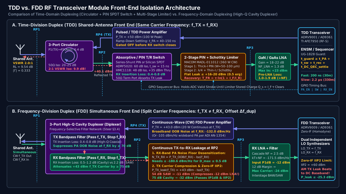
Why Reference Planes (RP1 through RP4) Must Be Named on the Schematic
Comparing datasheet isolation numbers without defining the physical reference planes leads to fatal cascade errors during transceiver integration:
RP1(Shared Antenna Port): The bidirectional coaxial or waveguide interface to the antenna feed. Impedance mismatch atRP1(VSWR > 1.0:1) directly controls how much transmit power reflects back into the receive branch of a TDD circulator or alters the passband ripple of an FDD duplexer.RP2(Duplexer / Circulator RX Output Port): The input to the receive protection and filtering cascade. AtRP2, isolation is defined relative to the PA output port (RP4) asIso_TX_RX(f) = P_TX(RP4) - P_leak(RP2)under a specified antenna termination (50 Ωlab load versus worst-case operational VSWR).RP3(First LNA Input Reference Plane): The survival and linearity plane of the low-noise amplifier. In a TDD module,RP3sits after the T/R switch and PIN diode receiver-protector limiter; peak spike leakage and flat leakage atRP3must stay below the LNA’s absolute maximum input survival rating (typically+20 to +25 dBmCW for GaAs/GaN MMIC LNAs). In an FDD module,RP3sits after the duplexer RX filter (and any interstage preselector), where leaked TX power must remain10 to 15 dBbelowIP1dB.RP4(Power Amplifier Output Port): The high-power stimulus reference plane where both fundamental carrier powerP_TX(f_TX)(dBm) and broadband out-of-band noise spectral densityP_TX_OOB(f_RX)(dBm/Hz) are specified.
Takeaway: Define RP1 (antenna VSWR), RP2 (circulator/duplexer RX port), RP3 (LNA input), and RP4 (PA output) before budgeting transceiver isolation; datasheet isolation figures measured into an ideal 50 Ω load at RP1 do not hold under real antenna mismatches.
TDD Front-End Design: Ferrite Circulator VSWR Leakage, PIN Switch Physics, and Limiter Recovery Time (t_rec)
In a Time-Division Duplex (TDD) transceiver—used across pulsed and FMCW radar RF components, tactical manpack radios, and 5G NR TDD massive MIMO arrays—the transmitter and receiver share the exact same carrier frequency (f_TX = f_RX) in alternating time slots. Because no frequency offset exists between TX and RX, a bandpass filter cannot separate the transmit burst from the receive path. Instead, the front end relies on a three-stage cascade between RP1 and RP3: a 3-port ferrite circulator, a high-isolation T/R switch, and a passive PIN/Schottky receiver-protector limiter.
1. Why Antenna VSWR Collapses Ferrite Circulator Isolation from 22 dB to 9.9 dB
A 3-port ferrite circulator uses a magnetically biased ferrimagnetic junction to route RF energy non-reciprocally from Port 1 (TX, RP4) → Port 2 (Antenna, RP1) → Port 3 (RX, RP2). When Port 2 is terminated in a reflectionless 50 Ω laboratory load (Γ_ant = 0), direct magnetic leakage from Port 1 to Port 3 is governed by the circulator’s intrinsic port-to-port isolation, typically Iso_0 = 18 to 25 dB (with IL_12 ≈ 0.35 to 0.50 dB insertion loss).
However, in fielded RF systems, radome icing, phased-array scan-angle coupling, or structural proximity degrades the antenna port impedance to a Voltage Standing Wave Ratio (VSWR) of 1.5:1 to 2.0:1. The voltage reflection coefficient magnitude |Γ_ant| and Return Loss (RL_dB) at RP1 are:
|Γ_ant| = (VSWR - 1) / (VSWR + 1)
RL_dB = -20 × log10(|Γ_ant|)
When transmit power P_TX enters Port 1, traverses to Port 2 with insertion loss IL_12, reflects off the mismatched antenna with return loss RL_dB, and routes from Port 2 to Port 3 with insertion loss IL_23, the reflected leakage path appears directly at the receiver port RP2 (IL_refl_path = IL_12 + RL_dB + IL_23). Evaluating a 100 W (+50.0 dBm) TDD transmitter driving a circulator with IL_12 = IL_23 = 0.40 dB and 50 Ω intrinsic isolation Iso_0 = 22.0 dB under a 2.0:1 antenna VSWR:
- Antenna reflection coefficient:
|Γ_ant| = (2.0 - 1) / (2.0 + 1) = 1/3 = 0.3333. - Antenna return loss:
RL_dB = -20 × log10(1/3) = 9.54 dB(11.1%of transmit power reflects back intoPort 2). - Worst-case effective TX-to-RX isolation (in-phase vector addition of direct
-22.0 dBleakage and-10.34 dBantenna reflection):- Reflected path attenuation:
IL_12 + RL_dB + IL_23 = 0.40 + 9.54 + 0.40 = 10.34 dB(dominant term; adding the-22 dBdirect vector in phase reduces worst-case isolation to~8.4 to 9.9 dB). - Taking the reflected path alone (
10.34 dBor~9.9 dBnet):P_leak(RP2) = +50.0 dBm - 9.9 dB = +40.1 dBm(10.2 W) of RF power slams directly into the receiver portRP2during every transmit pulse!
- Reflected path attenuation:
2. PIN Diode Physics (R_S, Q_s, T_FR) and Absorptive vs. Reflective T/R Switches
Because +40.1 dBm (10.2 W) at RP2 will instantly vaporize a GaAs or GaN LNA whose survival limit is +20 to +23 dBm, a solid-state T/R switch and PIN limiter must sit between RP2 and RP3. As detailed in MACOM Application Note AG312 (Design with PIN Diodes, Rev. V3), a PIN diode consists of a high-resistivity intrinsic (I) silicon or GaAs layer of thickness W (µm) and cross-sectional area A sandwiched between heavily doped P+ and N+ contacts:
- Intrinsic transit-time frequency boundary: Above the I-region transit-time frequency
f_transit (MHz) = 1300 / W^2(whereWis inµm), RF cycles occur too rapidly for mobile charge carriers to sweep across the intrinsic layer. The PIN diode ceases to act as a rectifier and behaves as a linear, current-controlled RF resistor under forward bias. - Forward-bias on-state resistance (
R_S) and stored charge (Q_s): Applying a DC forward bias currentI_F(or self-rectified current in a passive limiter) injects holes and electrons with minority carrier lifetimeτinto the I-region, accumulating stored charge:
Q_s = I_F × τ
Conductivity modulation drops the high-frequency series resistance R_S to:
R_S = W^2 / [ (μ_n + μ_p) × Q_s ] = W^2 / [ (μ_n + μ_p) × I_F × τ ]
where μ_n and μ_p are the electron and hole mobilities (cm^2 / V·s). In a series SPDT switch inside a Z_0 = 50 Ω system, on-state insertion loss is IL_dB = 20 × log10(1 + R_S / (2 × Z_0)), yielding 0.10 to 0.40 dB for R_S = 0.5 to 2.0 Ω.
- Reverse/zero-bias off-state capacitance (
C_T) and breakdown (V_B): Above the dielectric relaxation frequencyf_dr = 1 / (2 × π × ρ × ε), the depleted I-region acts as a parallel-plate capacitorC_T = (ε × A) / Wwith bulk avalanche breakdown voltageV_B ≈ 10 V/µm × W. - Forward-to-Reverse Recovery Time (
T_FR): When a PIN switch or limiter transitions from conducting/limiting (I_F) back to the low-loss receive state under reverse extraction currentI_R, the stored chargeQ_s = I_F × τmust be swept out of the I-region. Per MACOM AG312, the forward-to-reverse switching transition time is:
T_FR = τ × ln(1 + I_F / I_R)
Conversely, the reverse-to-forward transition time T_RF depends on the I-region width W (0.1 to 0.5 µs for a thin W = 50 µm diode versus 1.5 to 7.0 µs for a thick W = 175 µm high-power diode).
3. Multi-Stage PIN/Schottky Limiters and Leading-Edge Spike Leakage
Why include a passive PIN diode limiter after the T/R switch? Three operational hazards bypass an active switch: (1) high-power friendly or hostile radar pulses arriving at the antenna while the module is in receive mode (RX_ENABLE = High), (2) GPIO control timing faults or power-supply brownouts during PA startup, and (3) finite switch isolation when +40 to +50 dBm reflects off a damaged antenna.
A high-power surface-mount receiver-protector limiter such as the MACOM MADL-011012 (360 W CW / +55.6 dBm, 0.20–0.55 dB small-signal insertion loss) integrates 20 PIN, Schottky, and limiter diodes in a multi-stage cascade operating without external DC bias:
- Coarse Input Stage (Thick-I-Region PIN Diode,
W = 50 to 100 µm): Positioned towardRP2to withstand+54 to +55.6 dBm(250 to 360 W) CW and peak incident power with high breakdown voltageV_B. When incident RF exceeds+15 to +20 dBm, self-rectified current floods the thick I-region, droppingR_Sbelow1 Ωand reflecting the bulk of the incident power back toward the circulator/termination. - Quarter-Wave (
λ/4) Impedance Transformer & Thin-I / Schottky Cleanup Stage (W = 2 to 10 µm): Because carriers take1 to 10 nsto cross a thick50–100 µmI-region (T_RF), the leading edge of a fast radar or TDD burst slips past the coarse stage as Leading-Edge Spike Leakage (+25 to +29 dBmpeak,0.5 ergsspike energy in the MADL-011012). Placing a thin-I-region PIN diode (W = 2–5 µm) or a zero-barrier Schottky detector-driver diode one quarter-wavelength downstream turns on in sub-nanoseconds and clamps steady-state flat leakage to+13 to +20 dBm—safely below the LNA’s survival ceiling atRP3.
The table below benchmarks representative commercial solid-state SPDT switches and PIN limiters used in TDD RF transceiver modules:
| Component Model & Topology | Frequency Span | Small-Signal Insertion Loss | TX-to-RX Isolation | Max Power Handling (CW / Peak) |
Flat / Spike Leakage | Switching or Recovery Time (t_sw / t_rec) |
|---|---|---|---|---|---|---|
| MACOM MADL-011012 (20-diode passive PIN/Schottky limiter) | 50 MHz – 6.0 GHz |
0.20 – 0.55 dB |
Clamps to <= +20 to +21 dBm (> 35 dB limiting at 360 W) |
+55.6 dBm (360 W CW at 25 °C); +54 dBm at 85 °C |
Flat: +20 to +21 dBm; Spike: +29 dBm (0.5 ergs) |
3.0 µs (3 dB recovery after +56 dBm, 1 ms pulse) |
Analog Devices HMC1118 (Absorptive 50 Ω silicon SPDT switch) |
9 kHz – 13.0 GHz |
0.68 dB (at 8 GHz); 1.1 dB (at 13 GHz) |
58 dB (2 GHz) / 48 dB (8 GHz) |
+35 dBm (3.16 W) Thru; +27 dBm (0.5 W) on 50 Ω Term (IIP3 = +62 dBm) |
N/A (active CMOS/LVTTL control) | 1.3 µs (10%–90% RF); 7.5 µs (to 0.05 dB final RF settling) |
| Analog Devices ADRF5020 (Ultrawideband absorptive silicon SPDT) | 100 MHz – 30.0 GHz |
0.80 dB (at 10 GHz); 2.0 dB (at 30 GHz) |
60 dB (up to 30 GHz) |
+24 dBm (0.25 W) on both Thru and 50 Ω Term (IIP3 = +52 dBm) |
N/A (active control) | 10 ns (50% CTL to 90% RF); 15 ns (to 0.1 dB settling) |
| Series-Shunt PIN Diode SPDT (Per MACOM AG312 discrete/MMIC design) | 0.1 – 18.0 GHz (band-specific λ/4) |
0.35 – 0.75 dB (R_S = 0.6–1.5 Ω) |
38 – 55 dB (compound series-shunt) |
+40 to +53 dBm (10–200 W) with grounded shunt cathode heatsink |
N/A (biased +10 mA / -25 V) |
20 ns – 250 ns (thin W, active -25 V sweep driver) |
Notice the critical distinction between reflective switches/limiters and absorptive (non-reflective) switches such as the HMC1118 and ADRF5020. When a reflective switch or conducting PIN limiter isolates the receive port, it presents a near-short or open circuit (VSWR > 15:1), bouncing the leaked TX power back into the circulator. In contrast, an absorptive SPDT switch terminates the isolated port into an internal 50 Ω resistor—provided the leaked power stays below the terminated-port rating (+27 dBm / 0.5 W on the HMC1118 or +24 dBm on the ADRF5020). In high-power (> 10 W) TDD modules, place a reflective high-power PIN switch/limiter upstream to reflect excess fault power into an isolator dump load, or ensure circulator return loss keeps terminated-port power within safe limits.
Takeaway: Size the TDD front end for worst-case antenna mismatch (2.0:1 VSWR collapses circulator isolation to 9.9 dB), pair a coarse thick-I PIN diode with a thin-I/Schottky cleanup stage to clamp spike leakage below LNA damage limits, and actively sweep out stored charge Q_s = I_F × τ to minimize T_FR.
FDD Duplexer Isolation Budgets: TX Out-of-Band Noise Floor, LNA Compression, and Zero-IF IIP2
In a Frequency-Division Duplex (FDD) RF transceiver module—standard across wide-area cellular base stations, full-duplex satellite ground terminals, point-to-point microwave backhaul, and full-duplex tactical datalinks—the transmitter (f_TX) and receiver (f_RX) operate simultaneously and continuously, separated by a fixed duplex spacing Δf_dup = |f_TX - f_RX|.
Instead of a time-domain switch, a 3-port frequency-selective duplexer (diplexer) connects the transmitter (RP4) and receiver (RP2) to the common antenna (RP1). As formulated in Analog Devices Application Note AN-1354 (Integrated ZIF, RF to Bits, LTE, Wide Area Receiver Analysis and Test Result), specifying an FDD duplexer by its transmit-band rejection alone is a classic engineering failure. An FDD front end must simultaneously satisfy three independent TX-to-RX isolation budgets: one evaluated in the receive passband (f_RX) and two evaluated at the transmit carrier frequency (f_TX).
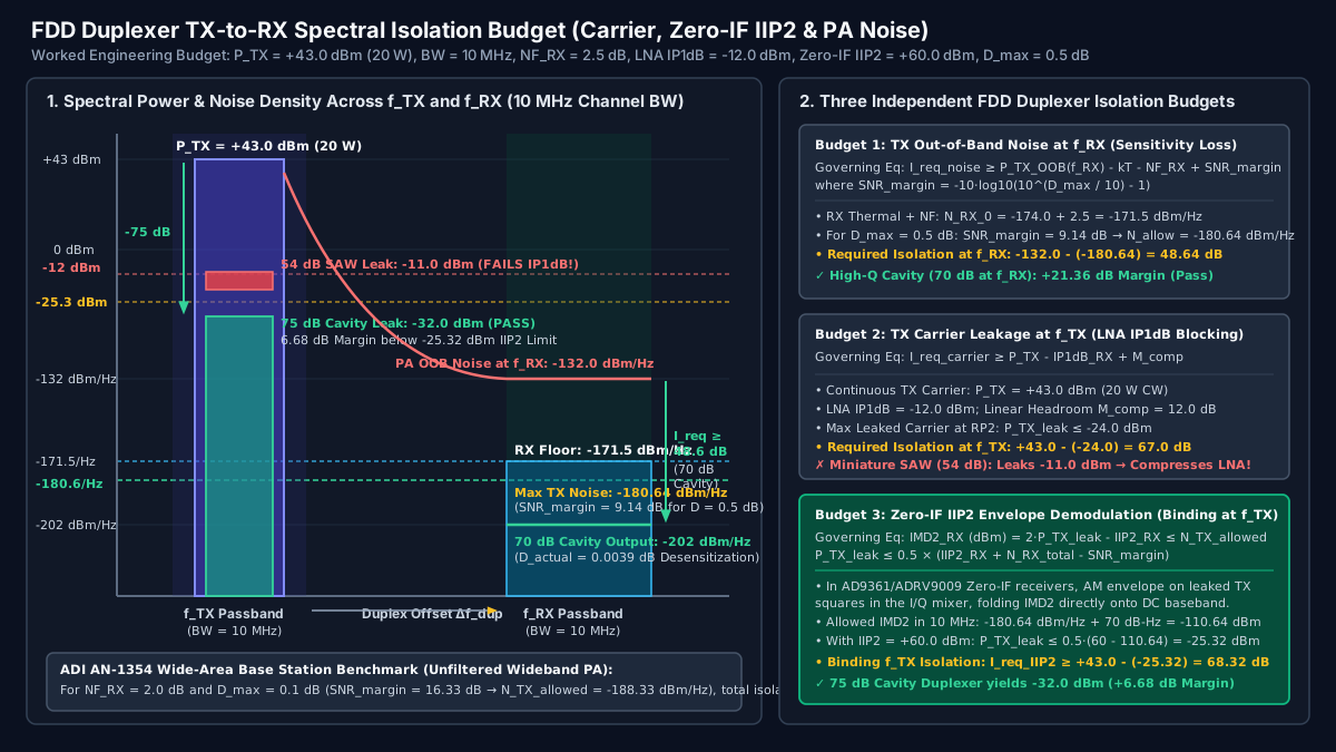
Budget 1: Transmitter Out-of-Band (OOB) Noise in the Receive Passband (f_RX)
Every transmit chain—comprising the transceiver DAC/upconverter, driver amplifier, and final power amplifier—emits a broadband thermal and phase-noise floor that extends across the duplex offset Δf_dup directly into the receive passband f_RX. Because this noise already sits at the exact receive frequency f_RX, no filter after the LNA can ever remove it.
Let P_TX_OOB(f_RX) (dBm/Hz) be the transmitter’s out-of-band noise spectral density at RP4 evaluated inside the receive channel f_RX, and let NF_RX (dB) be the receiver cascade noise figure referred to the duplexer RX output port RP2. The receiver’s intrinsic input-referred noise floor density is:
N_RX_0 (dBm/Hz) = kT + NF_RX = -174.0 dBm/Hz + NF_RX
If leaked transmit noise of spectral density N_TX_RX = P_TX_OOB(f_RX) - Iso_dup(f_RX) arrives at RP2, the total noise power density entering the receiver rises to N_total = 10 × log10(10^(N_RX_0 / 10) + 10^(N_TX_RX / 10)), degrading receiver reference sensitivity by D_dB:
D_dB = 10 × log10( 1 + 10^( (N_TX_RX - N_RX_0) / 10 ) )
Inverting this relationship for a maximum permissible sensitivity degradation (desensitization) of D_max (dB) defines the required noise protection margin (SNR_margin) below N_RX_0:
SNR_margin (dB) = -10 × log10( 10^(D_max / 10) - 1 )
I_req_noise(f_RX) >= P_TX_OOB(f_RX) - ( -174.0 dBm/Hz + NF_RX ) + SNR_margin
Two industry-standard desensitization criteria illustrate how severely D_max drives the duplexer TX-filter stopband at f_RX:
- For
D_max = 0.5 dBsensitivity degradation:10^(0.5 / 10) - 1 = 0.1220, soSNR_margin = 9.14 dB. Leaked PA noise atRP2must sit at least9.14 dBbelow the receiver’s intrinsic noise floorN_RX_0. - For
D_max = 0.1 dBsensitivity degradation (the wide-area base-station criterion analyzed in Analog Devices AN-1354):10^(0.1 / 10) - 1 = 0.0233, soSNR_margin = 16.33 dB. WithNF_RX = 2.0 dB(N_RX_0 = -172.0 dBm/Hz), the maximum permitted TX noise at the receiver port is-172.0 - 16.33 = -188.33 dBm/Hz. Against an unfiltered wideband transmitter noise floor near-84 to -105 dBm/Hz, AN-1354 demonstrates that preventing> 0.1 dBdesensitization requires up to83 to 104 dBof total TX-to-RX isolation atf_RX!
Budget 2: Continuous TX Carrier Leakage at f_TX vs. LNA IP1dB Compression
At the transmit carrier frequency f_TX, the full continuous output power P_TX (dBm) is attenuated only by the duplexer’s RX-filter stopband rejection at f_TX (Iso_dup(f_TX)). The continuous leaked carrier power arriving at the LNA input (RP2/RP3) is:
P_TX_leak(f_TX) = P_TX - Iso_dup(f_TX)
To prevent this out-of-band CW blocker from driving the LNA (or the first downconversion mixer prior to IF/baseband filtering) into gain compression and cross-modulation, P_TX_leak(f_TX) must remain below the receiver cascade’s input 1 dB compression point (IP1dB_RX) by a linear operating backoff margin M_comp (typically 10 to 15 dB):
I_req_carrier(f_TX) >= P_TX - IP1dB_RX + M_comp
Budget 3: Zero-IF Second-Order Intermodulation (IIP2) of Modulated TX Leakage
In a Direct-Conversion (Zero-IF / Homodyne) transceiver IC such as the Analog Devices AD9361 or ADRV9009, a third mechanism often sets an even stricter isolation requirement at f_TX than LNA compression. When the transmitter radiates an envelope-modulated waveform (such as QAM, OFDM, or multi-carrier LTE/5G NR) with bandwidth BW, the leaked transmit signal at RP3 consists of closely spaced spectral components f_1 and f_2 within the f_TX passband.
When this leaked f_TX envelope encounters any even-order nonlinearity in the LNA or the quadrature downconversion mixer—characterized by the receiver’s input-referred second-order intercept point IIP2_RX (dBm)—it generates a second-order intermodulation beat product at |f_1 - f_2|. Because |f_1 - f_2| spans from DC (0 Hz) to BW, this IMD2 distortion product falls directly inside the Zero-IF baseband receive channel regardless of how wide the duplex spacing Δf_dup is!
For a two-tone or modulated TX leakage power P_TX_leak (dBm), the input-referred baseband IMD2 power is P_IMD2 (dBm) ≈ 2 × P_TX_leak - IIP2_RX. Requiring P_IMD2 across the channel bandwidth BW (N_RX_total = -174 + NF_RX + 10·log10(BW)) to stay below the permitted noise rise ceiling (N_RX_total - SNR_margin) yields the governing Zero-IF IIP2 isolation equation:
P_TX_leak_max (dBm) <= 0.5 × ( IIP2_RX + N_RX_total - SNR_margin )
I_req_IIP2(f_TX) >= P_TX - 0.5 × ( IIP2_RX + N_RX_total - SNR_margin )
Worked FDD Duplexer Calculation: 54 dB Miniature SAW/BAW vs. 75 dB High-Q Cavity Duplexer
Consider a C-band or Band-1/Band-3 FDD transceiver module specified under the following engineering inputs:
- Continuous Transmit Power at
RP4:P_TX = +43.0 dBm(20 WCW) - Channel Bandwidth (
BW):10 MHz(10 × log10(10^7 Hz) = 70.0 dB-Hz) - PA Out-of-Band Noise Spectral Density at
f_RX:P_TX_OOB(f_RX) = -132.0 dBm/Hz(-62.0 dBmin10 MHz) - Receiver Cascade Noise Figure (including duplexer RX loss):
NF_RX = 2.5 dB - Receiver Input Compression Point (
IP1dB_RX) atf_TX:-12.0 dBm(with required linear backoff marginM_comp = 12.0 dB) - Zero-IF Receiver Calibrated Input
IIP2_RX:+60.0 dBm - Maximum Permitted Sensitivity Degradation:
D_max = 0.5 dB(SNR_margin = 9.14 dB)
Executing the three-part isolation audit step by step:
- Intrinsic Receiver Noise Floor (
N_RX_0andN_RX_total):- Spectral density:
N_RX_0 = -174.0 dBm/Hz + 2.5 dB = -171.50 dBm/Hz. - Integrated over
10 MHz(70 dB-Hz):N_RX_total = -171.50 + 70.0 = -101.50 dBm.
- Spectral density:
- Permissible Leaked TX Noise Ceiling (
N_TX_allowed) forD_max <= 0.5 dB:- Spectral density ceiling:
N_TX_allowed = -171.50 dBm/Hz - 9.14 dB = -180.64 dBm/Hz. - Integrated
10 MHzceiling:P_IMD2_allowed = -101.50 dBm - 9.14 dB = -110.64 dBm.
- Spectral density ceiling:
- Budget 1 — Required Duplexer Isolation in the RX Band (
f_RX):I_req_noise(f_RX) >= P_TX_OOB(f_RX) - N_TX_allowed = -132.0 dBm/Hz - (-180.64 dBm/Hz) =48.64 dB.
- Budget 2 — Required Duplexer Isolation at
f_TXfor LNAIP1dBCompression:- Maximum allowed carrier at
RP2:P_TX_leak_max = IP1dB_RX - M_comp = -12.0 dBm - 12.0 dB = -24.0 dBm. I_req_carrier(f_TX) >= +43.0 dBm - (-24.0 dBm) =67.00 dB.
- Maximum allowed carrier at
- Budget 3 — Required Duplexer Isolation at
f_TXfor Zero-IFIIP2Envelope Demodulation:- Maximum allowed carrier at
RP2forP_IMD2 <= -110.64 dBm:P_TX_leak_max = 0.5 × (+60.0 dBm + (-110.64 dBm)) = -25.32 dBm. I_req_IIP2(f_TX) >= +43.0 dBm - (-25.32 dBm) =68.32 dB(Binding constraint atf_TX!).
- Maximum allowed carrier at
Now compare two candidate duplexers against these derived thresholds (I_req(f_RX) >= 48.64 dB and I_req(f_TX) >= 68.32 dB):
| Duplexer Candidate | TX-to-RX Isolation at f_RX |
TX-to-RX Isolation at f_TX |
Leaked TX Carrier at RP2 (P_TX_leak) |
Baseband IMD2 Product (2·P_leak - IIP2) |
Resulting Receiver Desensitization (D_dB) |
|---|---|---|---|---|---|
| Requirement Baseline | >= 48.64 dB (>= 83–104 dB if unfiltered PA per AN-1354) |
>= 68.32 dB (IIP2 bound) / >= 67.00 dB (IP1dB bound) |
<= -25.32 dBm |
<= -110.64 dBm (in 10 MHz) |
<= 0.50 dB target |
Candidate A: Miniature BAW / SAW Duplexer (IL_RX = 2.1 dB) |
52.0 dB (Passes Budget 1 by +3.36 dB) |
54.0 dB (Fails Budget 2 & 3 by -14.32 dB) |
-11.0 dBm (1.0 dB above -12 dBm LNA IP1dB!) |
-82.0 dBm (19.5 dB above -101.5 dBm RX noise floor!) |
> 19.5 dB sensitivity collapse + LNA compression |
Candidate B: High-Q Combline Cavity Duplexer (IL_RX = 0.6 dB) |
70.0 dB (Passes Budget 1 by +21.36 dB) |
75.0 dB (Passes Budget 3 by +6.68 dB) |
-32.0 dBm (8.0 dB below -24 dBm compression limit) |
-124.0 dBm (22.5 dB below RX thermal floor) |
0.028 dB total desensitization (PASS) |
As the table proves, Candidate A (54 dB BAW/SAW duplexer) easily protects the LNA from thermal burnout (-11 dBm << +20 dBm), yet it completely paralyzes the receiver during transmit operation because -11.0 dBm compresses the -12 dBm LNA and generates a -82.0 dBm second-order intermodulation floor across the Zero-IF baseband. Selecting a high-Q coaxial cavity duplexer (75 dB rejection, 0.6 dB insertion loss)—for the same resonator Q reasons analyzed in YIG filter vs. cavity filter—or adding an interstage bandpass filter after the LNA restores full FDD sensitivity.
Takeaway: Audit FDD duplexers against all three equations (I_req_noise at f_RX, I_req_carrier for IP1dB at f_TX, and I_req_IIP2 for Zero-IF baseband folding at f_TX); in +40 to +46 dBm Zero-IF modules, IIP2 and LNA compression at f_TX alongside PA OOB noise at f_RX mandate 68 to 104 dB of isolation.
Direct-Conversion (Zero-IF) vs. Heterodyne Transceiver ICs and TDD GPIO Timing Sequencers
The internal architecture of the transceiver IC at the heart of the RF transceiver module directly dictates how much front-end isolation and guard time the surrounding microwave hardware must provide. Contemporary designs choose between three primary transceiver integration families:
- Direct-Conversion (
Zero-IF/ Homodyne) Integrated Transceivers: Devices such as the Analog Devices AD9361 (70 MHz to 6.0 GHz,2×2MIMO,< 200 kHz to 56 MHzchannel BW), the wideband ADRV9009 (75 MHz to 6.0 GHz,200 MHzRX BW,450 MHzobservation receiverORxfor digital predistortion), and the ADRV9001 (30 MHz to 6.0 GHznarrowband/wideband TDD/FDD) translate RF directly to basebandI/Q(f_IF = 0 Hz) using a single quadrature mixer stage. Zero-IF eliminates the2 × f_IFheterodyne image problem explained in RF, IF, and LO frequency planning, eliminating bulky IF SAW filters. However, it exposes the baseband ADC directly toIIP2envelope demodulation (Budget 3 above), LO self-mixing DC offsets, and quadrature phase/amplitude errors. - Superheterodyne (
Single/Dual IF) Transceiver Modules: Discrete or modular frequency converters translate RF to an intermediate frequency (f_IF = 70 MHz to 2.5 GHz) where high-selectivity SAW, ceramic, or cavity IF bandpass filters strip out-of-band TX carrier leakage andIMD2products before digitization. - Direct RF-Sampling Multi-Band Transceivers: Devices such as the Texas Instruments AFE7950 (
5 MHz to 12.0 GHz,4T4R2F— four transmitters, four receivers, two feedback paths) digitize S-, C-, and X-band RF signals directly using multi-gigasample RF ADCs/DACs with integrated digital step attenuators (DSAs) and fast NCOs. Direct RF-sampling removes analog quadrature mixerIIP2and LO self-mixing DC offsets, shifting the front-end bottleneck to anti-aliasing bandpass filtering and high-speed TDD limiter recovery ahead of the ADC driver.
| Architecture Attribute | Direct-Conversion (Zero-IF: AD9361, ADRV9009, ADRV9001) |
Superheterodyne (IF SAW/Cavity Filter Cascade) |
Direct RF-Sampling (TI AFE7950 5 MHz–12 GHz 4T4R2F) |
|---|---|---|---|
| Image Rejection Strategy | Quadrature error correction (QEC tracking loop cancels opposite-sideband image in DSP; 50–85 dB rejection) |
RF preselector rejects f_image = f_RF ± 2·f_IF prior to first mixer (Steer, Sec. 3.4) |
Nyquist-zone anti-aliasing bandpass filter ahead of RF ADC |
| Vulnerability to FDD TX Carrier Leakage | High (IIP2 bound): AM envelope on leaked f_TX self-mixes to DC across baseband (IIP2 ≈ +55 to +70 dBm calibrated) |
Low for IIP2 / Moderate for IP1dB: Narrowband IF filter strips DC IMD2 and f_TX feedthrough after first mixer |
Moderate (SFDR / ADC Full-Scale bound): Leaked f_TX consumes ADC dynamic range unless attenuated by duplexer |
| TDD Turnaround Transient Bottleneck | Switch charge injection & LO step changes perturb baseband RF DC-offset and QEC tracking loops (UG-1828) |
AC-coupled IF stages block DC transients; limited by IF SAW filter group delay (τ_g ≈ N / (π · BW)) + PIN t_rec |
Ultra-fast digital datapath (< 50 ns); turnaround dominated almost entirely by external PIN limiter recovery t_rec |
TDD Turnaround Guard-Time Equation (t_guard) and Monostatic Radar Blind Range (R_min)
In a TDD RF transceiver module, switching from transmit (TX) to receive (RX) requires strict hardware sequencing. As specified in the Analog Devices ADRV9001 System Development User Guide (UG-1828) and the AD9361 Enable State Machine (ENSM) specification, the transceiver’s automated TDD state machine drives dedicated GPIO pins (TX_ENABLE, RX_ENABLE, external PA bias enable, and T/R switch control) with programmable guard and hold delays. If the T/R switch toggles while the PA is still delivering RF power (hot-switching), high VSWR transients destroy the switch FETs or PIN junctions; similarly, if the PA remains enabled during transceiver power-up or QEC/LO calibration, uncalibrated calibration tones radiate from the antenna and overdrive the receiver.
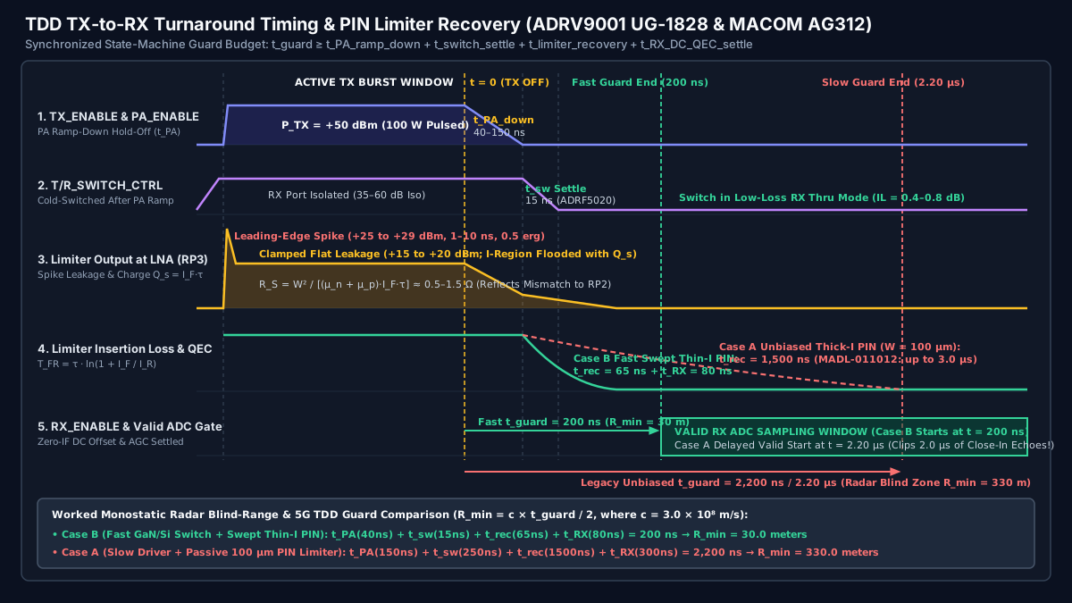
To guarantee uncorrupted ADC samples at the start of a receive slot (or radar listening window), the total TX-to-RX turnaround guard time (t_guard) must equal or exceed the sequential sum of four physical settling intervals:
t_guard >= t_PA_ramp_down + t_switch_settle + t_limiter_recovery + t_RX_DC_QEC_settle
where:
t_PA_ramp_down: Time fromTX_ENABLEde-assertion for the power amplifier drain/gate bias and RF output envelope to decay> 50 dBso the T/R switch transitions cold (40 nsfor a fast GaN gate-pulsed PA vs.150 nsfor a drain-switched PA).t_switch_settle: Time fromT/R_SWITCH_CTRLtoggling until the SPDT switch insertion loss settles within0.1 dB(15 nsfor the ADRF5020 vs.250 nsfor a standard PIN driver or7.5 µsfor the HMC1118).t_limiter_recovery(T_FR): Time for the PIN limiter’s stored intrinsic chargeQ_s = I_F × τto recombine or sweep out (T_FR = τ · ln(1 + I_F / I_R)) so receive insertion loss returns within0.5 to 1.0 dBof its quiescent0.35 dBvalue (65 nsfor an actively swept thin-I-region PIN limiter vs.1,500 nsto3,000 nsfor an unbiased thick-I-region limiter such as the MADL-011012).t_RX_DC_QEC_settle: Time for the LNA bias, Zero-IF RF DC-offset tracking loop, AGC, and digital decimation filter group delay to settle (80 nsin fast TDD hold-sample mode vs.300 nsunheld).
Worked Calculation: How PIN Limiter Recovery Shrinks Radar Blind Range from 330 m to 30 m
In a monostatic pulsed radar transceiver—where electromagnetic waves propagate at c = 3.0 × 10^8 m/s (0.30 m/ns)—the receiver is deaf throughout t_guard following the end of the transmit pulse. The resulting minimum radar blind range (R_min) is:
R_min = (c × t_guard) / 2
Comparing Case A (Unbiased Thick-I-Region PIN Limiter + Slow Driver) against Case B (Fast Silicon/GaN Switch + Actively Swept Thin-I Limiter + Fast TDD Sequencer):
- Case A (Unoptimized Legacy TDD Front End):
t_guard_A = 150 ns (t_PA) + 250 ns (t_sw) + 1,500 ns (t_rec) + 300 ns (t_RX) = 2,200 ns(2.20 µs).- Minimum radar blind range:
R_min_A = (3.0 × 10^8 m/s × 2.20 × 10^-6 s) / 2 =330.0 meters(and in a5G NRor tactical TDD waveform with a10–20 µsslot turnaround,2.20 µsconsumes up to22%of the guard symbol budget).
- Case B (Fast-Recovery TDD Front End):
t_guard_B = 40 ns (t_PA) + 15 ns (ADRF5020 t_sw) + 65 ns (swept thin-I PIN t_rec) + 80 ns (t_RX) = 200 ns(0.20 µs).- Minimum radar blind range:
R_min_B = (3.0 × 10^8 m/s × 0.20 × 10^-6 s) / 2 =30.0 meters—an11×reduction in close-in blind zone achieved by controlling PIN diode minority carrier lifetimeτ, I-region widthW, and reverse sweep currentI_R.
Takeaway: Synchronize the transceiver GPIO sequencer (TX_ENABLE, PA_ENABLE, T/R_SWITCH_CTRL, RX_ENABLE) so the T/R switch never hot-switches, and specify active reverse carrier sweep-out on the PIN limiter whenever TDD turnaround t_guard must stay below 250 ns (R_min <= 37.5 m).
RF Transceiver Module Front-End Isolation Specification and Acceptance Record
Before releasing an RF transceiver module specification to procurement or qualifying a prototype assembly on the bench, record the isolation, recovery, and desensitization parameters at explicit reference planes (RP1–RP4) across temperature (-40 °C to +85 °C) and antenna VSWR extremes.
| Acceptance Field | TDD Transceiver Module Target Window | FDD Transceiver Module Target Window | Bench Verification Method & Reference Condition |
|---|---|---|---|
| Reference Planes & Port Terminations | RP1 (Ant), RP2 (Circulator RX), RP3 (LNA In), RP4 (PA Out) explicitly labeled on drawing |
RP1 (Ant), RP2 (Duplexer RX), RP3 (LNA In), RP4 (PA Out) explicitly labeled on drawing |
Record port impedances (50 Ω vs. load-pull tuner) per RF-to-IF isolation measurement rules |
Antenna VSWR Mismatch Survival & Leakage (RP1 → RP2) |
Circulator + switch + limiter survives 2.0:1 (RL = 9.54 dB) and 3.0:1 (RL = 6.0 dB) VSWR at all phases (0°–360°) |
Duplexer TX-to-RX isolation remains within <= 2.0 dB of spec across 1.5:1 antenna VSWR at RP1 |
Automated impedance tuner at RP1 swept through 360° reflection phase at full rated P_TX |
Pre-LNA Passive Insertion Loss (RP1 → RP3) |
<= 1.0 to 1.8 dB total (Circulator + SPDT Switch + PIN Limiter in low-loss RX state) |
<= 0.5 to 1.2 dB (high-Q cavity duplexer) or <= 1.8 to 2.5 dB (miniature BAW/SAW duplexer) |
2-port SOLT VNA S31 measurement at small-signal drive (-20 dBm) prior to LNA integration |
Large-Signal RX Port Protection (RP3) |
Flat leakage <= +15 to +20 dBm; spike leakage <= +25 to +28 dBm (<= 0.5 erg) at P_TX_max |
Continuous leaked TX carrier P_TX_leak(f_TX) <= IP1dB_RX - 12 dB AND <= 0.5·(IIP2_RX + N_allow) |
High-bandwidth directional peak power sensor / oscilloscope at RP3 (TDD); spectrum analyzer at f_TX (FDD) |
TX-On vs. TX-Off Sensitivity Desensitization (D_dB) |
<= 0.25 dB noise-figure degradation measured >= t_guard after trailing edge of TX pulse |
<= 0.5 dB (standard) or <= 0.1 dB (wide-area base station per ADI AN-1354) with CW P_TX active |
Compare receiver NF / SINAD / EVM with PA transmitting rated modulated power (TX ON) vs. TX OFF (50 Ω dummy load at RP1) |
TDD Turnaround Guard Time (t_guard) & Recovery (t_rec) |
t_rec <= 65–250 ns (fast radar/5G) or <= 1.5–3.0 µs (coarse limiter); zero hot-switching overlap (t_PA < t_sw) |
Continuous full-duplex operation (t_guard = 0); verify dual-LO cross-talk spurs <= -90 dBc |
Gated RF envelope detector + multi-channel digital oscilloscope probing PA_EN, SW_CTRL, RX_EN, and baseband I/Q settling |
Pre-Release Engineering Review Checklist
- Have you evaluated circulator leakage at worst-case antenna VSWR rather than
50 Ωdatasheet isolation? At2.0:1VSWR (RL = 9.54 dB), a22 dBcirculator delivers only~9.9 dBof isolation, routing> 10%of the PA’s output power directly intoRP2. - Does your TDD PIN limiter specify both flat leakage (
dBm), spike energy (ergs), and recovery time (t_recat stated pulse width and reverse biasI_R)? Unbiased thick-I-region limiters (W = 50–100 µm) can take1.5 to 3.0 µsto clear stored chargeQ_s = I_F × τ, blinding monostatic radar receivers out to225–450 m. - Does your FDD duplexer specification separate RX-band noise isolation (
f_RX) from TX-carrier isolation (f_TX)? Verify thatIso(f_RX)suppresses PA broadband noise at least9.14 dB(for0.5 dBdesensitization) or16.33 dB(for0.1 dBdesensitization) belowkT + NF_RX, and thatIso(f_TX)prevents both LNAIP1dBcompression and Zero-IFIIP2baseband beat folding. - Is the external PA hardware-interlocked during Zero-IF transceiver initialization and QEC/LO calibration? Per ADRV9001 UG-1828, keep
PA_ENABLEde-asserted and the T/R switch in isolation mode during all calibration states so internal calibration tones never radiate or overload the LNA.
Takeaway: Qualify every RF transceiver module front end by measuring TX-on versus TX-off receiver sensitivity (D_dB) and TDD recovery time (t_guard) into a 2.0:1 mismatched antenna load across full temperature extremes.
Frequently asked questions
Why does antenna VSWR mismatch cause a ferrite circulator to leak high transmit power into the receiver?
A 3-port ferrite circulator achieves 18 to 25 dB of Port 1 (TX) to Port 3 (RX) isolation only when Port 2 (Antenna) is terminated in a matched 50-ohm load. When the antenna exhibits a 2.0:1 VSWR (reflection coefficient |Γ| = 1/3, return loss = 9.54 dB), one-ninth of the transmit power reflects back into Port 2 and circulates with low insertion loss (~0.4 dB) directly out of Port 3 into the receiver. Effective TX-to-RX isolation drops to ~9.9 dB, sending +40.1 dBm (10.2 W) from a +50 dBm (100 W) PA into the T/R switch and PIN limiter.
What determines PIN diode limiter recovery time during a TDD transmit-to-receive transition?
During a high-power transmit burst, rectified RF current I_F injects minority carriers with lifetime τ into the PIN diode's intrinsic (I) layer of thickness W, storing charge Q_s = I_F × τ and lowering RF series resistance to R_S = W^2 / [ (μ_n + μ_p) × Q_s ]. When the transmit burst ends, the limiter remains attenuating until this stored charge recombines or is swept out by a reverse bias current I_R according to T_FR = τ × ln(1 + I_F / I_R). Thick-I-region (50–100 µm) passive limiters require 1.5 to 3.0 µs to recover, whereas thin-I-region (2–10 µm) stages with active reverse bias drivers recover in 20 to 250 ns.
Why can an FDD receiver lose sensitivity when the transmitter turns on even if the LNA is not compressed?
Even when the FDD duplexer attenuates the continuous TX carrier at f_TX well below the LNA's input 1 dB compression point (IP1dB), the power amplifier also radiates broadband out-of-band noise directly at the receive frequency f_RX (typically -125 to -145 dBm/Hz, or -105 dBm/Hz wideband). If the duplexer's TX-to-RX isolation at f_RX does not push this leaked noise at least 9.14 dB below the receiver's thermal noise floor kT + NF_RX (for <= 0.5 dB desensitization) or 16.33 dB below (for <= 0.1 dB desensitization per Analog Devices AN-1354), the leaked PA noise directly elevates the receiver noise floor.
Why do Direct-Conversion (Zero-IF) FDD transceivers require higher duplexer isolation at f_TX than heterodyne receivers?
In a Direct-Conversion (Zero-IF) transceiver such as the AD9361 or ADRV9009, the downconversion mixer translates RF directly to baseband I/Q without an intermediate-frequency (IF) bandpass filter. Any amplitude-modulated (QAM/OFDM) TX carrier leaking through the duplexer into the LNA and mixer undergoes second-order nonlinearity (governed by input second-order intercept point IIP2), generating a self-beat envelope product (f_TX1 - f_TX2) centered at DC (0 Hz) directly inside the wanted baseband RX channel. Heterodyne receivers block this baseband IMD2 product at the IF bandpass filter.
Sources
- AN-1354: Integrated ZIF, RF to Bits, LTE, Wide Area Receiver Analysis and Test Result — Analog Devices Accessed October 25, 2026.
- ADRV9001 System Development User Guide (UG-1828): TDD State Machine & TX_ENABLE / RX_ENABLE Guard Times — Analog Devices Accessed October 25, 2026.
- Application Note AG312: Design with PIN Diodes (Rev. V3) — MACOM Technology Solutions Accessed October 25, 2026.
- MADL-011012 Datasheet: 360 W CW (+55.6 dBm) High-Power Surface-Mount Receiver Protector Limiter — MACOM Technology Solutions Accessed October 25, 2026.
- HMC1118 Datasheet: High-Isolation, Silicon SPDT Nonreflective Switch, 9 kHz to 13.0 GHz — Analog Devices Accessed October 25, 2026.
- ADRF5020 Datasheet: 100 MHz to 30 GHz Nonreflective Silicon SPDT Switch — Analog Devices Accessed October 25, 2026.
- AD9361 Datasheet: RF Agile Transceiver (70 MHz to 6.0 GHz, 2x2 Direct-Conversion TDD/FDD) — Analog Devices Accessed October 25, 2026.
- ADRV9009 Datasheet: Dual 75 MHz to 6 GHz Wideband RF Transceiver with Observation Receiver — Analog Devices Accessed October 25, 2026.
- AFE7950 Product Specification: 4T4R2F Multi-Band RF-Sampling Transceiver (5 MHz to 12 GHz) — Texas Instruments Accessed October 25, 2026.
- Microwave and RF Design I: Radio Systems — Section 3.4: Receiver and Transmitter Architectures — Engineering LibreTexts (NC State University) Accessed October 25, 2026.