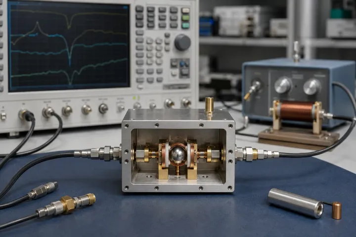
Direct answer
An RF synthesizer locks a Voltage-Controlled Oscillator (VCO) or YIG-Tuned Oscillator (YTO) to a reference clock across three primary PLL architectures. Integer-N PLLs (f_OUT = N · f_PFD) couple step size Δf to f_PFD, forcing N = 100,000 at 10 GHz for 100 kHz steps (+100 dB 20·log10(N) noise penalty, f_loop <= 5 kHz, and 931 µs settling). Fractional-N Sigma-Delta (Σ-Δ) PLLs (f_OUT = (N + K/M) · f_PFD, M = 2^24 to 2^39) decouple sub-hertz resolution from a 100–300 MHz PFD clock—cutting N to 100 at 10 GHz, lowering flat in-band PFD noise by 30 dB (-107 to -116 dBc/Hz), and shrinking hop lock time to 42.8 µs—while using charge-pump bleed current and f_PFD shifting to suppress Integer Boundary Spurs (IBS). Hybrid PLL + YTO synthesizers lock a YIG sphere (unloaded Q_u = 4,000–10,000) via an FM tickler coil to reach -138 dBc/Hz at 100 kHz and -152 dBc/Hz at 1 MHz offset at 10 GHz.
Key takeaways
- Fractional-N Sigma-Delta synthesis raises f_PFD from 100 kHz to 100 MHz at 10.0 GHz, cutting N from 100,000 to 100 and lowering flat in-band PFD phase noise by 30.0 dB (-77.0 to -107.0 dBc/Hz at FOM_PLL = -227 dBc/Hz).
- Widening loop bandwidth from f_loop = 5.0 kHz (100 kHz Integer-N) to f_loop = 200.0 kHz (100 MHz Fractional-N) reduces 100 MHz hop settling time (to ±100 Hz tolerance) from 931 µs down to 42.8 µs (25.3 µs with <2.5 µs VCO instant calibration).
- An L-th order MASH Sigma-Delta modulator shapes quantization noise upward at +20·(L - 1) dB/decade (+40 dB/dec for 3rd-order, +60 dB/dec for 4th-order), requiring a 3rd- or 4th-order loop filter with f_loop <= f_PFD / 20.
- Replacing an integrated SiGe/CMOS MMIC VCO (unloaded Q_u ≈ 20–50, -110 dBc/Hz at 100 kHz) with a Hybrid PLL + Dual-Coil YIG-Tuned Oscillator (Q_u = 4,000–10,000) improves 10 GHz far-out phase noise by 20–28 dB (-138 dBc/Hz at 100 kHz, -152 dBc/Hz at 1 MHz).
Selecting an RF synthesizer architecture for a microwave radar exciter, satellite communications block converter, electronic warfare (EW) receiver, or automated test instrument without accounting for feedback division ratio N causes severe close-in phase-noise degradation, reciprocal mixing sensitivity loss, or in-band spurious failure across the signal chain. Within the RF and microwave components hierarchy, an indirect PLL frequency synthesizer locks a tunable microwave oscillator to a precision quartz reference (OCXO or TCXO) across three distinct hardware topologies—Classical Integer-N PLLs, Fractional-N Multi-Stage Noise-Shaping (MASH) Sigma-Delta (Σ-Δ) PLLs, and Hybrid PLL + YIG-Tuned Oscillator (YTO) sources—to resolve the trade-off between channel step size (Δf), 20·log10(N) noise multiplication, and hop lock time (t_lock).
An RF synthesizer generates discrete programmable frequencies by locking a Voltage-Controlled Oscillator (VCO) or YIG-Tuned Oscillator (YTO) to a Phase Frequency Detector (PFD) comparison clock f_PFD. In an Integer-N PLL (f_OUT = N · f_PFD), the minimum channel step Δf equals f_PFD; synthesizing 10.0 GHz with 100 kHz channel steps forces f_PFD = 100 kHz, a feedback division ratio of N = 100,000 (+100.0 dB phase-noise multiplication), a narrow 5.0 kHz loop bandwidth, and a 931 µs settling time. A Fractional-N Sigma-Delta PLL (f_OUT = (N + K/M) · f_PFD, with modulus M = 2^24 to 2^39) decouples sub-hertz step size from f_PFD = 100 to 300 MHz, cutting N to 100 at 10.0 GHz, reducing flat in-band PFD phase noise by 30.0 dB (-77.0 to -107.0 dBc/Hz at FOM_PLL = -227 dBc/Hz), and accelerating 100 MHz hop lock time to 42.8 µs—while requiring charge-pump bleed current (I_bleed) and f_PFD frequency planning to suppress Integer Boundary Spurs (IBS). When system Reciprocal Mixing Dynamic Range (RMDR) requires wideband noise below integrated MMIC VCO limits (-110 dBc/Hz at 100 kHz), a Hybrid PLL + Dual-Coil YTO pairs fractional-N phase locking on a fast FM tickler coil with a single-crystal Y3Fe5O12 sphere (Q_u = 4,000–10,000) to reach -138 dBc/Hz at 100 kHz and -152 dBc/Hz at 1 MHz offset.
This architectural engineering reference extends the foundational five-block loop tutorial in how frequency synthesizers work and the direct-analog/DDS/PLL taxonomy in our microwave frequency synthesizers pillar guide. For register-level lock-detect timing versus settled RF frequency error, pair this analysis with HMC832 lock-detect frequency tolerance, single-sideband spectral integration in understanding phase noise, Kittel ferrimagnetic resonance in YIG sphere ferromagnetic resonance and Q-factor, and system-level carrier-to-noise degradation in the RF link budget calculation and fade margin guide.
| Architectural Parameter | Classical Integer-N PLL Synthesizer | Fractional-N MASH Sigma-Delta (Σ-Δ) PLL |
Hybrid PLL + Dual-Coil YIG-Tuned Oscillator (YTO) |
|---|---|---|---|
| Output Frequency & Feedback Equation | f_OUT = N · f_PFD (N integer counter) |
f_OUT = (N + K / M) · f_PFD (K ∈ [0, M-1], M = 2^24 to 2^39) |
Single-loop: f_YTO = (N + K/M) · f_PFD; Translation: f_YTO = M_harm · f_REF ± f_offset_PLL |
Minimum Channel Resolution (Δf) |
Δf = f_PFD (strictly coupled: 25 kHz or 100 kHz step forces f_PFD = 25 kHz or 100 kHz) |
Δf = f_PFD / M (decoupled: 0.0003 Hz to 6 Hz step at f_PFD = 100–300 MHz) |
Δf <= 0.001 Hz to 1 Hz (set by fractional-N or DDS offset loop via YTO FM tickler coil) |
Typical PFD Comparison Rate (f_PFD) |
10 kHz to 1 MHz (fine-step radio) or 50–250 MHz (coarse-step LO only) |
50 MHz to 300 MHz (100 MHz HMC832, 160 MHz ADF4371, 300 MHz LMX2594/LMX2820) |
50 MHz to 200 MHz in fine FM-coil PLL / offset loop (coarse DAC parks main coil within ±5 MHz) |
Feedback Division Ratio (N) at 10.0 GHz |
N = 100,000 (at Δf = 100 kHz) or N = 400,000 (at Δf = 25 kHz) |
N = 100 (at f_PFD = 100 MHz) or N = 50 (at f_PFD = 200 MHz) — 1,000× to 8,000× lower N |
N_eff = 1 to 100 (in harmonic-mixer offset loop) or N = 100 (in direct divided fractional loop) |
20·log10(N) Multiplication Penalty (10 GHz) |
+100.00 dB (N = 100,000) to +112.04 dB (N = 400,000) |
+40.00 dB (N = 100) to +33.98 dB (N = 50) — 60 to 78 dB lower N-multiplication |
0 dB to +40.00 dB inside FM-coil loop bandwidth (Giga-tronics AN-GT167A) |
In-Band Phase Noise (10 GHz, 10 kHz Offset) |
-77.0 dBc/Hz (f_PFD = 100 kHz) or -71.0 dBc/Hz (f_PFD = 25 kHz, FOM = -227) |
-107.0 dBc/Hz (FOM = -227, f_PFD = 100 MHz) to -116.0 dBc/Hz (FOM = -236 on LMX2594) |
-108 to -118 dBc/Hz at 10 kHz offset (tracking ultra-low-noise OCXO/comb reference + PLL) |
Wideband Phase Noise (10 GHz: 100 kHz / 1 MHz) |
-108 to -115 dBc/Hz @ 100 kHz; -130 to -135 dBc/Hz @ 1 MHz (MMIC VCO Q_u ≈ 20–50) |
-109 to -115 dBc/Hz @ 100 kHz; -132 to -136 dBc/Hz @ 1 MHz (ADF4371 / LMX2820 MMIC VCO) |
-132 to -142 dBc/Hz @ 100 kHz; -150 to -155 dBc/Hz @ 1 MHz (YIG Q_u = 4,000–10,000, 20–28 dB cleaner) |
Usable Closed-Loop Bandwidth (f_loop) |
1.25 kHz to 10 kHz (Gardner stability limit f_loop <= f_PFD / 10 to f_PFD / 20) |
100 kHz to 500 kHz (bounded by Σ-Δ high-pass quantization noise roll-off and VCO crossover) |
30 kHz to 200 kHz (bounded by YTO FM tickler coil 3 dB inductance limit and YIG crossover) |
Hop Settling Time (t_lock to ±100 Hz at 10 GHz) |
931 µs to 3.66 ms (slow analog loop settling across narrow 1.25–5 kHz bandwidth) |
25 µs to 60 µs (22.8 µs analog loop lock at f_loop = 200 kHz + 2.5–20 µs VCO sub-band LUT cal) |
2 ms to 10 ms for coarse main-coil step (> 50 MHz); 30–100 µs for fine FM-coil hop (< 10 MHz) |
| Dominant Spurious Mechanisms | Discrete PFD reference spurs at f_OUT ± k · f_PFD near the narrow loop passband |
Integer Boundary Spurs (IBS, -42 to -58 dBc unmitigated), fractional limit-cycle spurs, Σ-Δ noise hump |
Offset-mixer intermodulation cross-spurs (m·f_LO ± n·f_IF) and main-coil switching regulator ripple |
| SWaP & Representative Hardware | 5×5 mm to 7×7 mm QFN, 0.3–1.0 W (ADF4108, HMC704/ADF4371 in integer mode) |
5×5 mm to 7×7 mm QFN/LGA, 0.5–1.5 W (ADF4371, ADF4356, HMC832, LMX2594, LMX2595, LMX2820) |
30×30×20 mm to 50×50×25 mm magnetic cube + driver, 3.5–10 W (Micro Lambda YTO + PLL) |
Integer-N, Fractional-N Sigma-Delta, and Hybrid PLL+YIG RF Synthesizer Architectures
As established in Analog Devices Tutorial MT-086 (Fundamentals of Phase Locked Loops) and Dean Banerjee’s PLL Performance, Simulation, and Design, 5th Edition (SNAA106C), every indirect PLL frequency synthesizer is a negative-feedback control system that forces the divided output phase of a microwave oscillator to track a scaled reference oscillator. Inside the closed loop, an input reference divider (÷R, or reference multiplier ×M_ref) scales an external quartz reference f_REF (such as a 100 MHz Oven-Controlled Crystal Oscillator, OCXO) to produce the Phase Frequency Detector (PFD) comparison frequency:
f_PFD = f_REF × (M_ref / R)
The PFD compares rising edges of f_PFD against the feedback divider output f_FB = f_VCO / N_eff, driving a tri-state charge pump (I_CP) whose current pulses are integrated by the loop filter (Z_LF(s)) into the oscillator control voltage V_tune (or FM-coil current I_FM). While all three synthesizer classes share this feedback topology, the structure of the feedback divider N_eff and the unloaded quality factor (Q_u) of the microwave resonator partition them into three distinct performance regimes:
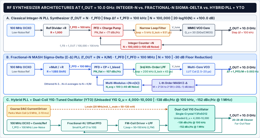
- Tier A — Classical Integer-N PLL (
f_OUT = N · f_PFD): The feedback path contains a synchronous pulse-swallow or dual-modulus counter (P / (P + 1)withAandBcounters, whereN = P · B + A) restricted to positive integersN ∈ ℤ. BecauseNcan only increment by1, the synthesizer’s minimum channel step is strictly locked to the PFD comparison rate (Δf = f_PFD). - Tier B — Fractional-N
MASHSigma-Delta (Σ-Δ) PLL (f_OUT = (N + K / M) · f_PFD): A high-speed digital Multi-Stage Noise-Shaping (MASH) Sigma-Delta modulator dynamically dithers a multi-modulus feedback divider across adjacent integer values (N - 3throughN + 4) on every cycle off_PFD. Over time, the average division ratio equalsN + K / M, whereMis the fractional modulus (2^24 = 16,777,216on the Analog Devices HMC832,2^32configurable on the Texas Instruments LMX2594 and LMX2820,2^38on the ADF4356, and2^39compound modulus on the ADF4371). This decouples sub-hertz channel tuning (Δf = f_PFD / M) fromf_PFD, allowingf_PFDto run at100 to 300 MHz. - Tier C — Hybrid PLL + Dual-Coil YIG-Tuned Oscillator (
YTO): Monolithic silicon/SiGe/BiCMOS VCO cores integrated inside single-chip wideband synthesizers use on-die spiral inductors and p-n varactors with low unloaded tank quality factors (Q_u ≈ 20 to 50), bounding their 10 GHz free-running phase noise to-109 to -115 dBc/Hzat100 kHzoffset. Replacing the MMIC VCO with a magnetically biased YIG oscillator—whose polished single-crystalY3Fe5O12sphere exhibits an unloadedQ_uof4,000 to 10,000per Micro Lambda Wireless YTO specifications—drops wideband phase noise at100 kHzand1 MHzoffsets by20 to 28 dB, while a fractional-N or offset-mixer PLL locks the YTO’s fast FM tickler coil.
Takeaway: Use Integer-N synthesis only when the frequency plan permits coarse steps equal to a high f_PFD (>= 50 MHz); select Fractional-N Sigma-Delta MMIC synthesizers for agile sub-hertz tuning with low close-in phase noise, and deploy Hybrid PLL+YTO architectures when receiver reciprocal mixing or radar clutter rejection demands < -135 dBc/Hz at 100 kHz offset at X-band.
The Integer-N Bottleneck: Why Narrow Channel Spacing Forces 20·log10(N) Noise and Slow Lock
To understand why classical Integer-N synthesis fails in fine-step microwave transceivers, follow the closed-loop phase transfer equations derived in Analog Devices MT-086 and Analog Dialogue PLLs for High-Frequency Receivers and Transmitters — Part 2.
1. The Δf = f_PFD Coupling Trap and 20·log10(N) Phase-Noise Multiplication
In an Integer-N frequency synthesizer, the locked output frequency is f_OUT = N · f_PFD. Suppose an X-band (f_OUT = 10.0 GHz) satellite or tactical radio requires a channel tuning step of Δf = 25 kHz or Δf = 100 kHz from a low-noise 100 MHz OCXO reference:
- For a
100 kHzchannel step: The reference divider must divide the100 MHzOCXO byR = 1,000down tof_PFD = 100 kHz. To reachf_OUT = 10.0 GHz, the feedback counter must divide byN = 10.0 GHz / 100 kHz = 100,000. - For a
25 kHzchannel step: The reference divider must divide byR = 4,000down tof_PFD = 25 kHz, forcingN = 10.0 GHz / 25 kHz = 400,000.
Inside the closed-loop bandwidth (f_m < f_loop), the feedback divider ÷N divides the VCO phase by N. For the PFD inputs to remain phase-locked, the closed loop multiplies any phase fluctuation originating at the reference input, reference divider, PFD, or charge pump by N in amplitude—which corresponds to N^2 in power spectral density, or:
ΔL_mult (dB) = 20 · log10(N)
At N = 100,000, the loop amplifies in-band PFD/charge-pump phase noise by +100.00 dB; at N = 400,000, the penalty reaches +112.04 dB. Using the industry-standard normalized PLL Flat Phase Noise Figure of Merit (FOM_PLL, typically -227 to -236 dBc/Hz) defined in Analog Dialogue Part 2, the flat in-band phase-noise floor PN_flat contributed by the PFD and charge pump is:
PN_flat (dBc/Hz) = FOM_PLL + 10 · log10(f_PFD / 1 Hz) + 20 · log10(N)
Even with a solid FOM_PLL = -227.0 dBc/Hz (characteristic of the Analog Devices HMC832 and ADF4356), evaluating PN_flat at 10.0 GHz for the 100 kHz Integer-N design gives -227.0 + 50.00 + 100.00 = -77.00 dBc/Hz (-70.98 dBc/Hz for the 25 kHz design)—rendering the local oscillator unusable for high-order QAM modulation or close-in Doppler radar processing.
2. The Gardner Discrete-Time Stability Boundary (f_loop <= f_PFD / 10)
The second casualty of a low f_PFD in an Integer-N rf synthesizer is the loop bandwidth f_loop. A digital PFD and charge pump do not operate in continuous time; they inject discrete correction current pulses once per period T_PFD = 1 / f_PFD. As derived in Dean Banerjee’s SNAA106C (Chapter 22), discrete sampling introduces excess phase lag Δφ_sample ≈ -ω · T_PFD / 2. If the unity-gain open-loop bandwidth f_loop approaches f_PFD, this sampling delay erodes phase margin and drives the closed loop into oscillation (Gardner’s stability limit):
f_loop <= f_PFD / 10 (absolute stability ceiling) and f_loop <= f_PFD / 20 (for robust 45°–60° phase margin and reference-spur suppression)
When f_PFD is pinned at 25 kHz or 100 kHz by an Integer-N channel plan, f_loop <= f_PFD / 20 restricts the usable loop bandwidth to 1.25 kHz or 5.0 kHz. This creates two compounding system penalties:
- Millisecond-scale frequency hopping: Because closed-loop transient settling time is inversely proportional to loop bandwidth (
t_lock ≈ 4.55 / f_loopfor a10^-6fractional frequency error step at damping factorζ = 0.707), a1.25 to 5.0 kHzloop requires0.91 ms to 3.64 msjust to settle the analog control voltage. - Unattenuated close-in VCO phase noise: The PLL only cleans up free-running VCO phase noise inside
f_m < f_loop. Whenf_loop = 5.0 kHz, the VCO’s steep1/f^3flicker-FM and1/f^2thermal phase noise between5 kHzand200 kHzoffset passes directly to the RF output without feedback suppression.
Takeaway: In an Integer-N PLL, narrow channel spacing (Δf = f_PFD) simultaneously inflates N (20·log10(N) = +100 to +112 dB at 10 GHz) and collapses loop bandwidth (f_loop <= f_PFD / 20 = 1.25–5 kHz), causing elevated close-in phase noise and millisecond settling times.
Fractional-N Sigma-Delta (Σ-Δ) Synthesis: Sub-Hz Resolution and High-f_PFD Noise Reduction
A Fractional-N PLL frequency synthesizer breaks the Δf = f_PFD deadlock by keeping the PFD comparison clock high (f_PFD = 100 to 300 MHz, often fed directly from the 100 MHz OCXO with R = 1 or multiplied by ×2) while synthesizing fractional division ratios inside the feedback path.
1. Multi-Modulus Divider Arithmetic and 24-Bit to 39-Bit Modulus Resolution
In a fractional-N loop (ADI MT-086), the feedback divider switches dynamically between integer moduli around N so that over M comparison cycles of f_PFD, the divider divides by N + 1 for K cycles and by N for M - K cycles (or across an 8-level multi-modulus span N - 3 to N + 4). The time-averaged output frequency and exact channel resolution Δf are:
f_OUT = ( N + K / M ) × f_PFD
Δf = f_PFD / M
Because M is implemented in digital CMOS logic inside the synthesizer IC, modern microwave synthesizers achieve sub-hertz or sub-millihertz frequency resolution even while operating at f_PFD = 100 to 300 MHz:
- Analog Devices HMC832 (
25 MHz to 3,000 MHz): Implements a24-bitfractional modulus (M = 2^24 = 16,777,216). Atf_PFD = 100 MHz, channel resolution isΔf = 100 MHz / 2^24 =5.96 Hz(2.98 Hzatf_PFD = 50 MHz). - Texas Instruments LMX2594 (
10 MHz to 15 GHz), LMX2595 (10 MHz to 20 GHz), and LMX2820 (45 MHz to 22.6 GHz): Implement a programmable32-bitfractional denominator (Mconfigurable up to2^32 - 1 = 4,294,967,295). Atf_PFD = 100 MHz, resolution reaches100 MHz / 2^32 =0.0233 Hz, and becauseMis arbitrarily programmable (not restricted to a power of two), the synthesizer can generate exact zero-error decimal channel steps (such asΔf = 100 kHzor1 Hz) with zero residual frequency rounding error. - Analog Devices ADF4356 (
53.125 MHz to 6.8 GHz) and ADF4371 (62.5 MHz to 32 GHz): TheADF4371cascades a25-bitfixed binary modulus (M_1 = 2^25 = 33,554,432) with a14-bitprogrammable auxiliary modulus (M_2 <= 16,383) for a combined39-bitfractional resolution:
f_VCO = [ INT + ( FRAC_1 + FRAC_2 / M_2 ) / 2^25 ] × f_PFD
At f_PFD = 100 MHz, the ADF4371 achieves a minimum frequency step of 100 MHz / 2^39 = 0.182 mHz (0.000182 Hz) with exact decimal channel synthesis.
2. MASH Sigma-Delta (Σ-Δ) High-Pass Quantization Noise Shaping (+20·(L - 1) dB/decade)
Early first-order fractional-N dividers toggled between N and N + 1 using a simple phase accumulator. Because the accumulator overflowed periodically at the fractional beat rate (K / M) · f_PFD, it injected a deterministic sawtooth phase error into the PFD, producing massive fractional spurs (-20 to -35 dBc).
Modern fractional-N synthesizers replace the simple accumulator with an L-th order Multi-Stage Noise-Shaping (MASH) Sigma-Delta (Σ-Δ) modulator (L = 1, 2, 3, or 4, user-selectable on the LMX2594 and LMX2820). A MASH modulator cascades L digital accumulators and feeds forward their quantized carry outputs through delay-differencing stages (1 - z^-1)^L. While the time-averaged division ratio remains strictly N + K / M, the deterministic fractional sawtooth is randomized into high-pass-shaped quantization phase noise whose single-sideband spectral density L_ΣΔ(f_m) follows (ADI MT-086 and TI SNAA106C, Chapter 14):
L_ΣΔ(f_m) = [ (2 · π)^2 / (12 · f_PFD) ] × [ 2 · sin( π · f_m / f_PFD ) ]^(2 · (L - 1)) / (2 · π · f_m / f_PFD)^2
For carrier offsets well below the PFD Nyquist frequency (f_m << f_PFD / π, so 2 · sin(π · f_m / f_PFD) ≈ 2 · π · f_m / f_PFD), this transfer function simplifies to a power-law slope in f_m:
L_ΣΔ(f_m) ∝ ( f_m / f_PFD )^(2 · (L - 1)) ⇒ Slope = +20 · (L - 1) dB/decade
Evaluating the noise-shaping slope across modulator orders L:
- 1st-Order
Σ-Δ(L = 1):0 dB/decadeflat spectral slope, dominated by discrete periodic fractional tones. - 2nd-Order
MASH-1-1(L = 2):+20 dB/decadehigh-pass slope; suppresses close-in quantization noise while keeping high-offset peaking moderate. - 3rd-Order
MASH-1-1-1(L = 3, standard on HMC832, ADF4371, LMX2594):+40 dB/decadehigh-pass slope; pushes close-in quantization noise well below the PFD thermal floor while requiring at least a 3rd-order loop filter (-60 dB/decaderoll-off abovef_loop) so the net closed-loopΣ-Δcontribution rolls off at+40 - 60 = -20 dB/decadeoutsidef_loop. - 4th-Order
MASH-1-1-1-1(L = 4, selectable on LMX2594/LMX2820):+60 dB/decadehigh-pass slope; maximizes randomization of small fractional words near integer boundaries, but requires a 4th-order loop filter (-80 dB/decaderoll-off) andf_loop <= f_PFD / 25to prevent an out-of-band quantization noise hump around0.5 to 3 MHzoffset.
Takeaway: Match the analog loop filter order to the MASH Sigma-Delta modulator order (Order_LPF >= L) and maintain f_loop <= f_PFD / 20 so the loop filter’s -20 · Order_LPF dB/decade stopband roll-off overtakes the modulator’s +20 · (L - 1) dB/decade rising quantization noise skirt.
Worked 10 GHz Phase Noise and Lock-Time Calculation: Integer-N vs. Fractional-N vs. Hybrid PLL+YIG
To quantify the exact decibel and microsecond trade-offs across all three rf synthesizer architectures, we evaluate a unified X-band (f_OUT = 10.000000 GHz) local oscillator design requiring at least Δf <= 100 kHz channel resolution and executing a Δf_step = 100 MHz frequency hop (from 9.900 GHz to 10.000 GHz) settled to within Δf_tol = ±100 Hz (±0.01 ppm).
1. Governing In-Band Phase Noise Identity (30.0 dB Floor Reduction Proof)
As formulated in Analog Dialogue Part 2 (Modeling Phase Noise and Reference Spurs), total in-band synthesizer phase noise inside f_m < f_loop is the power sum of three terms: (1) the flat PFD/charge-pump noise floor (PN_flat), (2) the PLL 1/f flicker noise (PN_1/f), and (3) the multiplied reference oscillator noise (PN_ref_out):
PN_flat (dBc/Hz) = FOM_PLL + 10 · log10(f_PFD / 1 Hz) + 20 · log10(N)
Substituting N = f_OUT / f_PFD (20·log10(N) = 20·log10(f_OUT) - 20·log10(f_PFD)) into PN_flat reveals the fundamental PFD scaling law:
PN_flat (dBc/Hz) = FOM_PLL + 20 · log10(f_OUT / 1 Hz) - 10 · log10(f_PFD / 1 Hz)
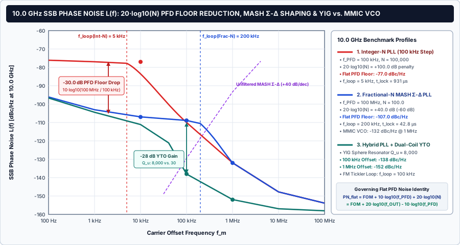
Look closely at what happens at f_OUT = 10.0 GHz (20·log10(10^10) = +200.00 dB-Hz) with a synthesizer IC having FOM_PLL = -227.0 dBc/Hz when moving from Integer-N (f_PFD = 100 kHz, N = 100,000) to Fractional-N (f_PFD = 100 MHz, N = 100):
- Reduction in
20·log10(N):20·log10(100) - 20·log10(100,000) = +40.00 dB - 100.00 dB =-60.00 dB. - Increase in
10·log10(f_PFD)(charge pump pulsing1,000×more often per second):10·log10(10^8) - 10·log10(10^5) = +80.00 dB - 50.00 dB =+30.00 dB. - Net flat PFD phase-noise reduction:
-60.00 dB + 30.00 dB = -10 · log10(100 MHz / 100 kHz) =-30.00 dB(PN_flatdrops from-77.00 dBc/Hzdown to-107.00 dBc/Hz, or down to-116.00 dBc/Hzon the TI LMX2594 / LMX2820 withFOM_PLL = -236.0 dBc/Hz)!
Next, evaluate the PLL 1/f flicker noise contribution at offset f_m = 10 kHz using normalized FOM_1/f = -126.0 dBc/Hz (ADF4371 datasheet, or -134.0 dBc/Hz on the LMX2820):
PN_1/f(f_m) = FOM_1/f + 20 · log10(f_OUT / 1 GHz) - 10 · log10(f_m / 10 kHz)
At f_OUT = 10.0 GHz (+20.0 dB relative to 1 GHz) and f_m = 10 kHz (0 dB relative to 10 kHz), PN_1/f(10 kHz) = -126.0 + 20.0 - 0 = -106.00 dBc/Hz. Power-summing PN_flat = -107.00 dBc/Hz, PN_1/f = -106.00 dBc/Hz, and the multiplied 100 MHz OCXO (-165 dBc/Hz + 40 dB = -125.0 dBc/Hz) gives the total Fractional-N phase noise at 10 kHz offset:
L_total(10 kHz) = 10 · log10( 10^(-10.70) + 10^(-10.60) + 10^(-12.50) ) = -103.42 dBc/Hz (-111.8 dBc/Hz on the LMX2820).
2. Governing Second-Order Transient Lock-Time Equation (t_lock)
Per Dean Banerjee (SNAA106C, Chapter 23), when a second-order Type-II PLL with natural frequency ω_n = 2 · π · f_n and damping factor ζ (0.707 critically damped optimal response) steps across a frequency jump Δf_step, the envelope of the instantaneous frequency error decays exponentially until it stays permanently inside the settling tolerance ±Δf_tol:
t_lock ≈ -ln( (Δf_tol / Δf_step) × sqrt(1 - ζ^2) ) / ( ζ × ω_n )
For a critically damped loop with ζ = 0.7071 (sqrt(1 - ζ^2) = 0.7071), the natural frequency f_n relates to the unity-gain open-loop bandwidth f_loop by f_n ≈ 0.700 × f_loop (ω_n = 2 · π · 0.700 · f_loop = 4.3982 · f_loop). Substituting our hop parameters Δf_step = 100 MHz (10^8 Hz) and Δf_tol = 100 Hz (Δf_tol / Δf_step = 10^-6):
- Logarithmic transient factor:
-ln( 10^-6 × 0.7071 ) = -ln( 7.071 × 10^-7 ) =14.1622. - Closed-form analog settling time vs.
f_loop:t_lock = 14.1622 / ( 0.7071 × 4.3982 · f_loop ) = 20.028 / ω_n =4.5537 / f_loop. - Total hop time (
t_total): In wideband multi-core MMIC VCOs (ADF4371, LMX2594), total hop time adds the digital VCO sub-band calibration intervalt_cal(~20 µswith LUT assist, or< 2.5 µswith LMX2820 Instant Calibration) tot_lock. In a Hybrid PLL+YTO, a coarse hop (> 50 MHz) adds the electromagnetic main-coil step and eddy-current decay timet_coil(~3.50 msper Micro Lambda Wireless YTO definitions).
The 9-step calculation matrix below compares four 10.0 GHz synthesizer implementations across identical reference and hop conditions:
| Calculation Step & Parameter | Integer-N (Δf = 25 kHz Step) |
Integer-N (Δf = 100 kHz Step) |
Fractional-N MASH Σ-Δ (M = 2^35) |
Hybrid PLL + Dual-Coil YTO |
|---|---|---|---|---|
1. Carrier f_OUT & Channel Step (Δf) |
10.000000 GHz (Δf = 25 kHz) |
10.000000 GHz (Δf = 100 kHz) |
10.000000 GHz (Δf = 0.003 Hz) |
10.000000 GHz (Δf < 0.01 Hz) |
2. PFD Frequency (f_PFD) & Divider (R) |
f_PFD = 25.0 kHz (R = 4,000) |
f_PFD = 100.0 kHz (R = 1,000) |
f_PFD = 100.0 MHz (R = 1) |
f_PFD = 100.0 MHz (in FM-coil loop) |
3. Feedback Ratio (N) & 20·log10(N) |
N = 400,000 (+112.04 dB) |
N = 100,000 (+100.00 dB) |
N = 100.0 (+40.00 dB, -60 dB vs. Int-N) |
N_eff = 100 (direct) or 4–20 (offset mixer) |
4. Pulse-Rate Term 10·log10(f_PFD) |
+43.98 dB-Hz |
+50.00 dB-Hz |
+80.00 dB-Hz |
+80.00 dB-Hz |
5. Flat PFD Floor (PN_flat, FOM = -227) |
-70.98 dBc/Hz |
-77.00 dBc/Hz |
-107.00 dBc/Hz (-116.0 on LMX2594) |
-107.0 to -118.0 dBc/Hz (in-band) |
6. Total In-Band Noise @ 10 kHz Offset |
-70.98 dBc/Hz (N-dominated) |
-76.99 dBc/Hz (N-dominated) |
-103.42 dBc/Hz (-111.8 on LMX2820) |
-110.0 to -118.0 dBc/Hz |
7. Far-Out Noise (100 kHz / 1 MHz Offsets) |
-110 dBc/Hz / -132 dBc/Hz |
-110 dBc/Hz / -132 dBc/Hz |
-109 dBc/Hz / -132 dBc/Hz (MMIC Q_u ≈ 30) |
-138 dBc/Hz / -152 dBc/Hz (YIG Q_u ≈ 8,000) |
8. Loop Bandwidth (f_loop) & ω_n |
1.25 kHz (ω_n = 5,498 rad/s) |
5.00 kHz (ω_n = 21,991 rad/s) |
200.0 kHz (ω_n = 879,646 rad/s) |
100.0 kHz (ω_n = 439,823 rad/s on FM coil) |
9. Hop Lock Time (100 MHz Step to ±100 Hz) |
3,663 µs (3.643 ms loop + 20 µs LUT) |
931 µs (911 µs loop + 20 µs LUT) |
42.8 µs (22.8 µs loop + 20 µs LUT; 25.3 µs on LMX2820) |
3,546 µs coarse (3.50 ms main coil + 45.5 µs FM loop); 45.5 µs fine |
Takeaway: At 10.0 GHz, switching from a 100 kHz Integer-N loop to a 100 MHz Fractional-N Sigma-Delta loop lowers the flat PFD noise floor by exactly 30.00 dB (-77.00 to -107.00 dBc/Hz) and cuts 100 MHz hop settling time by 21.7× (931 µs down to 42.8 µs).
Integer Boundary Spurs (IBS) and Fractional Spur Mitigation Techniques
The primary engineering trade-off of Fractional-N synthesis is the generation of Integer Boundary Spurs (IBS) and fractional sequence spurs. As analyzed in Analog Dialogue PLLs for High-Frequency Receivers and Transmitters — Part 3, understanding how these discrete tones form inside the IC package allows hardware designers to suppress them by 20 to 45 dB.
1. Physical Mechanism of Integer Boundary Spurs (f_spur = min(K/M, 1 - K/M) · f_PFD)
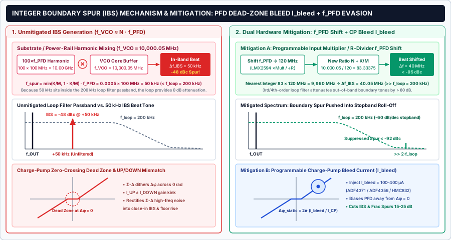
Suppose our 10.0 GHz Fractional-N synthesizer (f_PFD = 100.00 MHz) is tuned to f_VCO = 10,000.05 MHz—just 50 kHz above the 100th harmonic of f_PFD (100 × 100.00 MHz = 10,000.00 MHz, so N + K/M = 100.0005). Two physical coupling mechanisms occur simultaneously on the synthesizer die:
- Substrate and Power-Rail Harmonic Mixing: High-slew-rate CMOS/CML clock buffers in the reference path generate harmonics at
k · f_PFD(k = 100sits at10,000.00 MHz). This10.00 GHzclock harmonic couples across silicon substrate capacitance, bondwires, or sharedVDDpower rails into the VCO core or VCO divider input (10,000.05 MHz), intermodulating to produce a50 kHzbeat note:
f_spur_IBS = | f_VCO - N_nearest · f_PFD | = min( K / M , 1 - K / M ) × f_PFD
- PFD/Charge-Pump Turn-On Dead-Zone Nonlinearity: In an ideal linear charge pump, the high-frequency
MASH Σ-Δdither averages out in the loop filter. However, near zero phase error (Δφ ≈ 0), real PFD/charge-pump circuits exhibit a finite turn-on dead zone and a gain mismatch between theI_UP(PMOS source) andI_DOWN(NMOS sink) current mirrors. As theΣ-Δmodulator dithers the instant phase error back and forth acrossΔφ = 0at the slow beat rate50 kHz, this dead-zone kink rectifies (demodulates) the high-frequencyΣ-Δsequence directly into a50 kHzcurrent tone entering the loop filter.
Because f_spur_IBS = 50 kHz lies inside the f_loop = 200 kHz loop filter passband, the loop filter provides 0 dB of attenuation, allowing an unmitigated -42 to -58 dBc Integer Boundary Spur to appear on the 10.00005 GHz RF carrier!
2. Four-Vector Spur Mitigation Matrix
The engineering table below details the exact offset equations, coupling paths, and hardware mitigations for all four spurious families in a Fractional-N pll frequency synthesizer:
| Spur Category | Frequency Offset Equation | Physical Coupling Mechanism | Unmitigated Level | Hardware & Frequency-Planning Mitigation |
|---|---|---|---|---|
1. Fundamental Integer Boundary Spur (IBS) |
f_spur = |f_VCO - N_nearest · f_PFD| = min(K/M, 1 - K/M) · f_PFD |
VCO buffer leaks into PFD/reference harmonic N·f_PFD; PFD zero-crossing dead zone & I_UP ≠ I_DOWN mismatch demodulate the beat inside f_loop |
-42 to -58 dBc (when f_spur < f_loop, 0 dB filter rejection) |
1) Shift f_PFD via ÷R, ×2 doubler, or programmable input multiplier (×1–×7 on LMX2594) so f_spur >= 2.5 · f_loop; 2) Enable Charge-Pump Bleed Current I_bleed (100–400 µA on ADF4371 / ADF4356 / HMC832) to lock at static phase offset Δφ_static = 2π·(I_bleed / I_CP) away from Δφ = 0 |
| 2. Harmonic Integer Boundary Spur | f_spur = |m · f_VCO - k · f_PFD| (m = 2, 3 VCO harmonics vs. k · f_PFD) |
High-slew-rate CMOS/CML reference harmonics radiate via shared VDD_VCO / VDD_PFD rails or package bondwires when K/M ≈ 1/2, 1/3, 2/3, 1/4 |
-55 to -72 dBc (at fractional sub-harmonics 0.5, 0.333, 0.25) |
1) Separate LDO rails for VDD_VCO, VDD_CP, and VDD_DIG with ferrite beads + 100 pF / 10 nF / 4.7 µF decoupling; 2) Run VCO fundamental with output divider ÷D (D = 2, 4) so VCO core avoids half/third-integer multiples of f_PFD |
3. Σ-Δ Limit-Cycle & Quantization Hump |
L_ΣΔ(f_m) ∝ (f_m / f_PFD)^(2L-2); discrete tones when GCD(K, M) is large |
Short periodic Σ-Δ bitstreams create limit-cycle spurs; insufficient loop-filter order lets +40/+60 dB/dec noise peak at 0.3–2 MHz |
+6 to +15 dB phase-noise hump or -60 dBc limit-cycle tones |
1) Use 3rd/4th-order loop filter (>= 20·L dB/dec attenuation) with f_loop <= f_PFD / 20; 2) Seed Σ-Δ phase accumulator with non-zero dither or force K odd (co-prime GCD(K, M) = 1 on LMX2594) to maximize sequence period |
4. PFD Reference Spur (±k · f_PFD) |
f_spur = f_OUT ± k · f_PFD (k = 1, 2, 3...) |
Loop filter leakage I_leak or PFD reset pulses modulate V_tune at f_PFD, scaled by VCO gain K_VCO (MHz/V) |
-65 to -95 dBc (degrades by +20·log10(K_VCO)) |
1) Maximize f_PFD / f_loop ratio (f_PFD = 100 MHz with f_loop = 200 kHz gives f_PFD / f_loop = 500, placing spur 2.7 decades into stopband); 2) Use NP0/C0G loop filter capacitors and low-K_VCO multi-core VCOs |
3. Worked IBS Evasion and Charge-Pump Bleed (I_bleed) Calculation
Apply both hardware mitigations from the right panel of Figure 3 to our f_VCO = 10,000.05 MHz channel:
- Mitigation A — Reference Frequency Planning (
f_PFDShift): On the Texas Instruments LMX2594 or LMX2820, engage the integrated Programmable Input Multiplier (×3) and Reference Divider (÷2.5orR = 5with×6)—or changeRfrom1(f_PFD = 100 MHz) to shiftf_PFDto120.00 MHz(or80.00 MHz). Atf_PFD = 120.00 MHz, the new feedback ratio is10,000.05 MHz / 120.00 MHz = 83.33375. The nearest integer multiple off_PFDis83 × 120 MHz = 9,960.00 MHz, moving the fundamental boundary beat from50 kHzout toΔf_IBS = 40.05 MHz—which sits200×beyond the200 kHzloop filter cutoff where the 3rd-order loop filter attenuates it by> 60 dB(below-92 dBc)! - Mitigation B — Charge-Pump Bleed / Offset Current (
I_bleed) Sizing: Whenf_PFDcannot be shifted, enable the programmable charge-pump bleed current (Register0x09on the HMC832 or bleed registers on the ADF4371). For a main charge-pump current ofI_CP = 2.50 mAand a 3rd-orderMASH-1-1-1peak-to-peak phase excursion of4VCO cycles (±4 · 2π / N = ±0.08π radatN = 100), setting a constant bleed current ofI_bleed = 200 µA(8%ofI_CP, or3.9 µA × N_bleedper theADF4371datasheet formulaI_bleed / I_CP < 4 / N) forces the PFD to lock at a steady-state static phase offset:
Δφ_static = 2 · π × ( I_bleed / I_CP ) = 2 · π × ( 0.20 mA / 2.50 mA ) = 0.16 · π rad (28.8°)
Because Δφ_static = 0.16π rad exceeds the peak ±0.08π rad MASH Σ-Δ phase dither excursion, only the UP charge-pump switch ever turns on dynamically during locked operation—completely avoiding the zero-crossing dead zone and reducing in-band fractional and integer-boundary spurs by 15 to 25 dB.
Takeaway: Suppress Integer Boundary Spurs by combining automated f_PFD frequency planning (shifting f_PFD via ÷R or input multiplier whenever min(K/M, 1 - K/M) · f_PFD < 2.5 · f_loop) with a 100 to 400 µA charge-pump bleed current that biases the PFD out of its zero-crossing dead zone.
Hybrid PLL + YIG-Tuned Oscillator (YTO) Synthesizers: Bridging Resonator Q and Loop Agility
Even when a Fractional-N Sigma-Delta PLL reduces the close-in 10 kHz phase-noise floor at 10.0 GHz to -107 to -116 dBc/Hz, what sets the synthesizer’s phase noise at 100 kHz to 10 MHz carrier offsets—the region that governs receiver Reciprocal Mixing Dynamic Range (RMDR) in RF module transmitter and receiver cascades and RF, IF, and LO frequency planning?
1. Leeson’s Equation: Why Single-Crystal YIG (Q_u = 8,000) Beats Monolithic VCOs (Q_u = 30) by 20–28 dB
Outside the closed-loop bandwidth (f_m > f_loop), the loop filter attenuates PFD corrections and the synthesizer’s phase noise converges to the free-running oscillator phase noise L_VCO(f_m). According to Leeson’s phase-noise equation, an oscillator’s 1/f^2 thermal phase-noise skirt at offset f_m is inversely proportional to the square of the resonator’s unloaded quality factor (Q_u^2, or -20 · log10(Q_u)):
L_VCO(f_m) = 10 · log10( [ (F · k_B · T) / (2 · P_sig) ] × [ 1 + ( f_0 / (2 · Q_L · f_m) )^2 ] × ( 1 + f_c / f_m ) )
Compare the physical resonator inside a wideband silicon/SiGe MMIC synthesizer IC against a magnetically tuned YIG oscillator (detailed in YIG sphere ferromagnetic resonance and Q-factor and YIG oscillator vs. VCO vs. DRO):
- Monolithic Multi-Core MMIC VCO (ADF4371, LMX2594, LMX2820): Uses planar on-chip metal spiral inductors and semiconductor varactor/switched-capacitor banks with an unloaded tank quality factor of
Q_u ≈ 20 to 50. Scaled tof_0 = 10.0 GHz,L_VCOis bounded to-109 to -113 dBc/Hzat100 kHzoffset and-132 to -135 dBc/Hzat1 MHzoffset. - Single-Crystal Yttrium Iron Garnet (
Y3Fe5O12) Sphere Resonator (Micro Lambda Wireless YTO): Uses a0.25 to 0.50 mmoptically polished ferrimagnetic sphere with narrow ferrimagnetic resonance linewidth (ΔH ≈ 0.25 to 0.50 Oe), achieving an unloadedQ_u = 4,000 to 10,000across2 to 20 GHz. That150× to 250×higher resonatorQ_ureduces1/f^2phase noise at10.0 GHzto-135 to -142 dBc/Hzat100 kHzoffset and-150 to -155 dBc/Hzat1 MHzoffset—a20 to 28 dBimprovement in far-out spectral purity!
2. Dual-Coil YTO Control Loop and Offset-Mixer Translation Architecture
As explained in how YIG oscillators work, Micro Lambda Wireless YTO documentation, and Giga-tronics Application Note AN-GT167A (High Speed Wide Band Frequency Synthesis), a YIG oscillator tunes linearly with magnetic field (f_0 = γ · H_0, where γ = 2.8 MHz/Oe). Because the main electromagnet coil requires hundreds of turns around a laminated ferromagnetic pole piece, it exhibits high inductance (L_main = 50 to 120 mH), a high tuning sensitivity (K_main ≈ 15 to 25 MHz/mA), and a 3 dB small-signal modulation bandwidth below 1 to 5 kHz.
To phase-lock a YTO without triggering instability from the main coil’s inductive pole and eddy-current lag, a Hybrid PLL + YTO synthesizer splits frequency control across two physical coils:
- Main Tuning Coil (Coarse Open-Loop DAC Parking): A low-noise 16-to-20-bit DAC current source drives
I_main(100 to 800 mA) to park the YIG sphere within±2 to ±10 MHzof the target carrier. Following a large multi-gigahertz step, magnetic pole-piece settling and hysteresis recovery take2.0 to 10.0 ms. - FM Tickler Coil (Fast Closed-Loop PLL Phase Lock): A single- or few-turn air-core copper loop (
L_FM = 1 to 5 µH, sensitivityK_FM ≈ 200 to 500 kHz/mA, total capture range±20 to ±50 MHz) sits inside the pole gap directly adjacent to the YIG sphere, providing a3 dBmodulation bandwidth up to500 kHz to 2 MHz. The Fractional-N PLL (or harmonic comb-generator offset translation loop per AN-GT167A) drivesI_FMwith a closed-loop bandwidth off_loop = 50 to 150 kHz—wide enough to lock the YTO with sub-hertz accuracy and< 50 µsfine-hop settling, yet narrow enough that above150 kHzoffset the synthesizer inherits the YIG resonator’s-138 to -152 dBc/Hzphase-noise skirt.
3. Benchmark IC & Module Specification Matrix and Selection Checklist
The reference table below summarizes verified datasheet specifications for leading commercial rf synthesizer ICs and hybrid YTO assemblies:
| Device / Module | Frequency Coverage | Fractional Modulus (M) |
Max f_PFD (Int / Frac) |
Normalized FOM_PLL (Int / Frac) |
Normalized 1/f Flicker (FOM_1/f) |
10 GHz-Scaled Phase Noise (100 kHz / 1 MHz) |
Key Spur / Calibration Feature |
|---|---|---|---|---|---|---|---|
| ADI HMC832 | 25 MHz – 3.0 GHz |
24-bit (2^24 = 16.78M) |
100 MHz / 100 MHz |
-230 / -227 dBc/Hz |
-125 dBc/Hz |
-110 / -133 dBc/Hz (scaled from 3 GHz) |
Programmable CP offset (0 to ±795 µA in 15 µA steps) + Reg 0x07 digital LD window |
| ADI ADF4356 | 53.125 MHz – 6.8 GHz |
38-bit (2^24 × 2^14) |
250 MHz / 125 MHz |
-230 / -227 dBc/Hz |
-126 dBc/Hz |
-109 / -132 dBc/Hz (scaled from 6.8 GHz) |
Negative bleed current for IBS suppression + 4-core VCO |
| ADI ADF4371 | 62.5 MHz – 32.0 GHz |
39-bit (2^25 × 2^14) |
250 MHz / 160 MHz |
-234 / -231 dBc/Hz |
-126 dBc/Hz |
-109 / -132 dBc/Hz (-111 / -134 at 8 GHz) |
Integrated quadrupler to 32 GHz + 3.9 µA × N programmable CP bleed |
| TI LMX2594 / LMX2595 | 10 MHz – 15 GHz (20 GHz on 2595) |
32-bit configurable (1st–4th order MASH) |
400 MHz / 300 MHz |
-236 dBc/Hz |
-129 dBc/Hz |
-113.5 / -134.5 dBc/Hz (-110 at 15 GHz) |
Integrated Input Multiplier (×1–×7) for IBS evasion + JESD204B SYSREF sync |
| TI LMX2820 | 45 MHz – 22.6 GHz |
32-bit configurable (1st–4th order MASH) |
400 MHz / 300 MHz |
-236 dBc/Hz |
-134 dBc/Hz |
-113.0 / -135.5 dBc/Hz (-117.5 at 6 GHz) |
< 2.5 µs Instant Calibration VCO hopping + ultra-low -134 dBc/Hz 1/f noise |
| Hybrid PLL + Micro Lambda YTO | 2.0 GHz – 20.0 GHz (multi-octave) |
24-to-39-bit Fractional or DDS Offset |
50 MHz – 200 MHz (FM-coil loop) |
-230 to -236 dBc/Hz |
-128 to -134 dBc/Hz |
-138 dBc/Hz @ 100 kHz; -152 dBc/Hz @ 1 MHz |
Single-crystal Y3Fe5O12 (Q_u = 4,000–10,000) + dual-coil coarse/FM phase lock |
Use the following four-point engineering decision rules when specifying an rf synthesizer for a new transceiver or instrument frequency plan:
- Specify Fractional-N
MASH Σ-ΔMMIC Synthesizers (LMX2820,LMX2594,ADF4371) when the system requires sub-hertz to kilohertz channel steps,< 50 µshop settling, compact6×6 mmQFN footprint (< 1.5 WDC power), and integrated phase noise (10 kHz to 10 MHzRMS jitter< 45 to 70 fs) where-110 to -113 dBc/Hzat100 kHzoffset (10 GHz) meets the receiver’s blocker budget. - Specify Hybrid PLL + Dual-Coil YIG-Tuned Oscillator (
YTO) Modules when the local oscillator drives a wide-dynamic-range spectrum analyzer, EW receiver, or X/Ku-band Doppler radar where strong off-channel blockers at100 kHz to 5 MHzoffsets demand-135 to -152 dBc/Hzfar-out phase noise that no monolithic silicon VCO can achieve, and where2 to 10 mscoarse tuning (30–100 µswithin the±20 MHzFM-coil window) and4 to 8 Wcoil power fit the platform budget. - Mandate Automated
f_PFDEvasion and Charge-Pump Bleed (I_bleed) in every Fractional-N frequency table: computef_spur_IBS = min(K/M, 1 - K/M) · f_PFDfor every target channel and automatically toggle the reference divider÷Ror input multiplier (×M_ref) whenever a channel lands within2.5 · f_loopof an integer multiple off_PFD. - Separate Digital Lock Detect (
LD) from Settled RF Frequency Tolerance: As proven in HMC832 lock-detect frequency tolerance and TDD vs. FDD transceiver front-end timing, always budget both the digital VCO sub-band calibration time (t_cal) and the analog loop settling time (t_lockto a stated±Δf_tolin Hz) in the system switching timeline.
Takeaway: Match the synthesizer resonator (MMIC VCO vs. YIG sphere) to the receiver’s 100 kHz–10 MHz reciprocal mixing requirement, and size f_PFD, MASH modulator order, and loop bandwidth f_loop to bound close-in 20·log10(N) phase noise and switching time.
Frequently asked questions
Why does a Fractional-N PLL achieve 30 dB lower in-band phase noise than an Integer-N PLL at the same output frequency?
Flat in-band PLL phase noise follows PN_flat = FOM_PLL + 10·log10(f_PFD) + 20·log10(N). Because N = f_OUT / f_PFD, substituting N yields PN_flat = FOM_PLL + 20·log10(f_OUT) - 10·log10(f_PFD). At f_OUT = 10.0 GHz with a 100 kHz channel step, an Integer-N PLL must run at f_PFD = 100 kHz (N = 100,000, +100 dB multiplication). A Fractional-N Sigma-Delta PLL synthesizes the same 100 kHz (or sub-hertz) step while running at f_PFD = 100 MHz (N = 100, +40 dB multiplication). The 1,000x reduction in N saves 60 dB while the 1,000x increase in PFD comparison rate adds 30 dB of pulse-rate scaling, yielding a net 30.0 dB reduction in flat in-band phase noise.
What causes Integer Boundary Spurs (IBS) in a Fractional-N RF synthesizer and how are they suppressed?
Integer Boundary Spurs occur when the VCO frequency f_VCO (or a harmonic m·f_VCO) approaches an integer multiple N·f_PFD of the PFD clock—meaning the fractional modulus word K/M approaches 0 or 1. The divided VCO edge sweeps slowly across the reference edge at the beat frequency f_spur = min(K/M, 1 - K/M) · f_PFD. When f_spur falls inside the PLL loop bandwidth f_loop, substrate/power-rail harmonic leakage and PFD/charge-pump turn-on dead-zone nonlinearity demodulate this beat tone without loop-filter attenuation (-42 to -58 dBc). Engineers suppress IBS by shifting f_PFD via an input reference divider or multiplier (such as the x1-to-x7 multiplier on the TI LMX2594) so the beat moves outside 2·f_loop, and by applying a programmable charge-pump bleed current (100–400 µA on the ADI ADF4371, ADF4356, or HMC832) to bias the PFD away from its zero-crossing dead zone.
How does MASH Sigma-Delta modulator order affect loop filter design in a Fractional-N synthesizer?
An L-th order Multi-stage noise Shaping (MASH) Sigma-Delta modulator dithers the instant feedback division ratio across N - 3 to N + 4 so that time-averaged division equals N + K/M while shaping quantization phase noise out of the close-in passband at a high-pass slope of +20·(L - 1) dB/decade (+20 dB/decade for 2nd-order, +40 dB/decade for 3rd-order MASH-1-1-1, and +60 dB/decade for 4th-order MASH-1-1-1-1). To prevent this rising high-offset quantization noise from creating an out-of-band phase-noise hump between 300 kHz and 5 MHz, the analog loop filter must include at least L poles (a 3rd- or 4th-order filter rolling off at -60 to -80 dB/decade) with closed-loop bandwidth f_loop kept at or below f_PFD / 20.
Why do Hybrid PLL + YIG-Tuned Oscillator (YTO) synthesizers use two separate tuning coils?
A YIG-tuned oscillator relies on a DC magnetic field H_0 across a pole gap to tune a single-crystal Y3Fe5O12 sphere at 2.8 MHz/Oe. Generating a 2 to 20 GHz magnetic field requires a multi-hundred-turn main electromagnet coil with high inductance (50 to 120 mH) and a 3 dB modulation bandwidth below 5 kHz (2 to 10 ms step settling due to magnetic pole-piece eddy currents and hysteresis). Closing a wideband PLL directly around the main coil would cause loop instability. Hybrid PLL+YTO synthesizers therefore drive the main coil with a low-noise coarse DAC current source to park the carrier within ±2 to ±10 MHz, while closing a 50 to 200 kHz PLL loop around a low-inductance (1 to 5 µH) single-turn FM tickler coil mounted directly adjacent to the YIG sphere.
Why does VCO sub-band autocalibration add to the total hop time of a wideband Fractional-N MMIC synthesizer?
To achieve low VCO tuning sensitivity K_VCO (15 to 40 MHz/V)—which minimizes varactor thermal noise modulation and PFD reference spurs—integrated wideband synthesizers such as the ADI ADF4371 (62.5 MHz to 32 GHz) and TI LMX2594/LMX2820 divide their octave-spanning VCO range into multiple VCO cores and 128 to 256 switched-capacitor sub-bands. When commanded to a new frequency, a digital finite state machine must first select the correct VCO core and capacitor bank (taking 20 to 200 µs in standard autocalibration, or <2.5 µs using pre-stored look-up tables and Instant Calibration on the LMX2820) before the analog charge-pump loop settles across its 20 to 45 µs transient.
Sources
- MT-086 Tutorial: Fundamentals of Phase Locked Loops (PLLs) — Analog Devices Accessed October 25, 2026.
- PLLs for High-Frequency Receivers and Transmitters — Part 2: Modeling Phase Noise and Reference Spurs — Analog Devices (Analog Dialogue) Accessed October 25, 2026.
- PLLs for High-Frequency Receivers and Transmitters — Part 3: Fractional-N Spurs, Integer Boundary Spurs, and Mitigation — Analog Devices (Analog Dialogue) Accessed October 25, 2026.
- ADF4371 Datasheet: Microwave Wideband Synthesizer with Integrated VCO (62.5 MHz to 32 GHz) — Analog Devices Accessed October 25, 2026.
- ADF4356 Datasheet: Microwave Wideband Synthesizer with Integrated VCO (53.125 MHz to 6.8 GHz) — Analog Devices Accessed October 25, 2026.
- HMC832 Datasheet: Fractional-N PLL with Integrated VCO, 25 MHz to 3000 MHz — Analog Devices Accessed October 25, 2026.
- LMX2594 Datasheet: 10-MHz to 15-GHz Wideband RF Synthesizer with Phase Synchronization and JESD204B Support — Texas Instruments Accessed October 25, 2026.
- LMX2595 Datasheet: 10-MHz to 20-GHz Wideband RF Synthesizer with Integrated VCO — Texas Instruments Accessed October 25, 2026.
- LMX2820 Datasheet: 45-MHz to 22.6-GHz Wideband RF Synthesizer with Phase Synchronization — Texas Instruments Accessed October 25, 2026.
- PLL Performance, Simulation, and Design, 5th Edition (SNAA106C) — Texas Instruments (Dean Banerjee) Accessed October 25, 2026.
- Technology Description: YIG Tuned Oscillators (Resonator Q, Dual-Coil Tuning, and Phase Noise) — Micro Lambda Wireless Accessed October 25, 2026.
- Application Note AN-GT167A: High Speed Wide Band Frequency Synthesis — Giga-tronics Accessed October 25, 2026.